Home > Press > Versatile Dual Function Sample Preparation System For SEM
 |
Abstract:
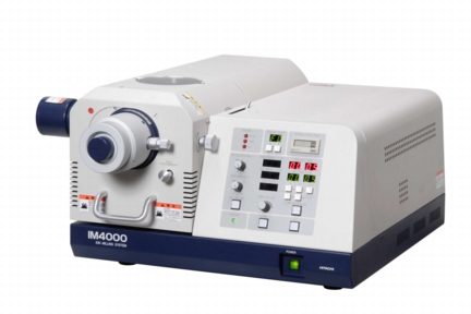
Hitachi High-Technologies has launched the IM4000 Ion Milling system. Used to prepare specimens for scanning electron microscope (SEM) imaging and analytical studies such as EDX and EBSP, the versatile IM4000 is capable of both pin-point cross-section and flat surface ion milling. Cross-section milling provides smooth cross-section specimens for high resolution imaging of subsurface structures, with the cross section position accurately controllable by fine positioning of a beam-shielding mask edge. Flat milling provides uniform polishing of surfaces of 5 mm diameter or more with variable angle milling, to either flatten surfaces or to selectively enhance specimen surface features (relief milling).
Versatile Dual Function Sample Preparation System For SEM
Maidenhead, UK | Posted on August 31st, 2011The two IM4000 applications - Cross section and flat surface milling - are realised via 2 different removable sample stage units, allowing for convenient specimen setting and cutting edge definition using an external optical microscope.
The IM4000 ion milling system features a new high-current Argon ion gun that delivers cross sectional milling rates of 300μm/hr in Silicon for dramatically reduced cross-sectioning times. The wide Argon ion beam can define sharp cross sections even on samples of dissimilar materials with different hardness that can not be cut or broken without causing material deformations or dislocations. Sensitive materials like polymers or papers can be processed by freely selecting proper lower ion beam energies between 0 and 6kV, without need for special sample cooling.
Wide and smooth flat milled surfaces of approximately 5mm in diameter or more can be achieved within minutes by shifting the centre of the defocused ion beam from the sample rotation or swinging centre. The beam irradiation angle to the specimen surface is selectable from 0� to 90�. This makes the IM4000 useful in a multitude of different fields and applications such as materials, semiconductors, research and quality control.
####
For more information, please click here
Contacts:
Press Enquiries:
Denis Bulgin
In Press Public Relations Ltd
PO Box 24
Royston, Herts, SG8 6TT
Tel: +44 (0)1763 262621
www.inpress.co.uk
Other Enquiries:
High-Technologies Corporation
Whitebrook Park, Lower Cookham Road
Maidenhead, Berkshire SL6 8YA.
Tel: + 44 (0) 800 316 1500
Copyright © Hitachi High-Technologies Corporation
If you have a comment, please Contact us.Issuers of news releases, not 7th Wave, Inc. or Nanotechnology Now, are solely responsible for the accuracy of the content.
Bookmark:


| Related News Press |
News and information
![]() Simulating magnetization in a Heisenberg quantum spin chain April 5th, 2024
Simulating magnetization in a Heisenberg quantum spin chain April 5th, 2024
![]() NRL charters Navy�s quantum inertial navigation path to reduce drift April 5th, 2024
NRL charters Navy�s quantum inertial navigation path to reduce drift April 5th, 2024
![]() Discovery points path to flash-like memory for storing qubits: Rice find could hasten development of nonvolatile quantum memory April 5th, 2024
Discovery points path to flash-like memory for storing qubits: Rice find could hasten development of nonvolatile quantum memory April 5th, 2024
Imaging
![]() Nanoscale CL thermometry with lanthanide-doped heavy-metal oxide in TEM March 8th, 2024
Nanoscale CL thermometry with lanthanide-doped heavy-metal oxide in TEM March 8th, 2024
![]() The USTC realizes In situ electron paramagnetic resonance spectroscopy using single nanodiamond sensors November 3rd, 2023
The USTC realizes In situ electron paramagnetic resonance spectroscopy using single nanodiamond sensors November 3rd, 2023
![]() Observation of left and right at nanoscale with optical force October 6th, 2023
Observation of left and right at nanoscale with optical force October 6th, 2023
Announcements
![]() NRL charters Navy�s quantum inertial navigation path to reduce drift April 5th, 2024
NRL charters Navy�s quantum inertial navigation path to reduce drift April 5th, 2024
![]() Discovery points path to flash-like memory for storing qubits: Rice find could hasten development of nonvolatile quantum memory April 5th, 2024
Discovery points path to flash-like memory for storing qubits: Rice find could hasten development of nonvolatile quantum memory April 5th, 2024
Tools
![]() Ferroelectrically modulate the Fermi level of graphene oxide to enhance SERS response November 3rd, 2023
Ferroelectrically modulate the Fermi level of graphene oxide to enhance SERS response November 3rd, 2023
![]() The USTC realizes In situ electron paramagnetic resonance spectroscopy using single nanodiamond sensors November 3rd, 2023
The USTC realizes In situ electron paramagnetic resonance spectroscopy using single nanodiamond sensors November 3rd, 2023
|
|
||
|
|
||
| The latest news from around the world, FREE | ||
|
|
||
|
|
||
| Premium Products | ||
|
|
||
|
Only the news you want to read!
Learn More |
||
|
|
||
|
Full-service, expert consulting
Learn More |
||
|
|
||