Home > Press > UDE-Researchers produce high-quality graphene
 |
Abstract:
Professor Michael Horn-von Hoegen at the Center for Nanointegration (CeNIDE) at the University Duisburg-Essen (UDE) has developed a process capable of producing a high-quality product with a single step.
UDE-Researchers produce high-quality graphene
Germany | Posted on June 7th, 2011Graphene is the electronic miracle material of the 21st century. Until now, only sheets that were very small or of a somewhat inferior quality could be produced that were too small or not well suited for high-tech applications. Now, however, Professor Michael Horn-von Hoegen at the Center for Nanointegration (CeNIDE) at the University Duisburg-Essen (UDE) has developed a process capable of producing a high-quality product with a single step. The results of his research have been published in the journal �Applied Physics Letters� (Vol.98, No. 14)
The difference in scale between graphene�s thickness and that of a sheet of paper can be compared to the difference between that same piece of paper and the height of the Bosphorus Bridge in Istanbul. Graphene conducts electricity like no other material in the world and it is extremely resilient. Until recently, it had one major flaw which could not be taken lightly: the consensus among researchers around the world was it would never exist in a stable format. Nevertheless, in 2004 the Russian scientists Andre Geim and Konstantin Novoselov succeeded in producing graphene, for which they received the Nobel Prize in Physics in 2010. UDE also has a number of projects that explore this miracle material.
Graphene is comprised of a honeycomb carbon structure only a single atom thick�no material can be thinner than that. Of course, it is extremely laborious to produce larger sheets of the material. Even when it does work the quality of the product leaves much to be desired. This is where the research from Professor Horn-von Hoegen�s experimental physics group comes into play. He states, �Our goal is to understand the growth of the sheet in detail, so that we can develop a �recipe� for producing graphene that is free from defects, as large as possible, and suitable for industrial applications.�
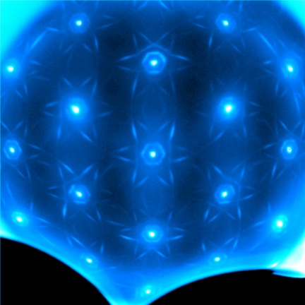
He developed the recently-published procedure in collaboration with researchers from the universities of Cologne and Twente: Ethylene gas is used as a catalyst on the surface of an iridium crystal to produce a carbon layer that is exactly one single atom thick. Horn-von Hoegen�s team tested the quality of the product themselves, directly following fabrication, using high resolution low energy electron diffraction (LEED). The LEED immediately reveals defects as star shaped structures. Horn-von Hoegen explained, �They may look pretty, but they indicate that the individual carbon honeycomb structures are distorted. For that reason we are delighted when the diffraction images don�t reveal any stars�they�re boring, but they�re perfect.�
Graphene is regarded as the only two-dimensional solid object in the world. Within it, electrons move faster than in any other substance, which attests to its extreme conductivity. In battery technology, particularly given the rapidly growing interest in electric cars, the prospect of a super-conductive membrane between the battery�s poles is especially promising. It could even replace silicon in a future generation of computers and greatly increase processing capabilities, enabling many more computations at a faster speed. This would only be possible with high-quality graphene, which makes the work of the UDE professor particularly critical.
####
For more information, please click here
Contacts:
Birte Vierjahn
Copyright © CeNIDE, University of Duisburg-Essen
If you have a comment, please Contact us.Issuers of news releases, not 7th Wave, Inc. or Nanotechnology Now, are solely responsible for the accuracy of the content.
Bookmark:


| Related News Press |
News and information
![]() Simulating magnetization in a Heisenberg quantum spin chain April 5th, 2024
Simulating magnetization in a Heisenberg quantum spin chain April 5th, 2024
![]() NRL charters Navy�s quantum inertial navigation path to reduce drift April 5th, 2024
NRL charters Navy�s quantum inertial navigation path to reduce drift April 5th, 2024
![]() Discovery points path to flash-like memory for storing qubits: Rice find could hasten development of nonvolatile quantum memory April 5th, 2024
Discovery points path to flash-like memory for storing qubits: Rice find could hasten development of nonvolatile quantum memory April 5th, 2024
Graphene/ Graphite
![]() NRL discovers two-dimensional waveguides February 16th, 2024
NRL discovers two-dimensional waveguides February 16th, 2024
Chip Technology
![]() Discovery points path to flash-like memory for storing qubits: Rice find could hasten development of nonvolatile quantum memory April 5th, 2024
Discovery points path to flash-like memory for storing qubits: Rice find could hasten development of nonvolatile quantum memory April 5th, 2024
![]() Utilizing palladium for addressing contact issues of buried oxide thin film transistors April 5th, 2024
Utilizing palladium for addressing contact issues of buried oxide thin film transistors April 5th, 2024
![]() HKUST researchers develop new integration technique for efficient coupling of III-V and silicon February 16th, 2024
HKUST researchers develop new integration technique for efficient coupling of III-V and silicon February 16th, 2024
Nanoelectronics
![]() Interdisciplinary: Rice team tackles the future of semiconductors Multiferroics could be the key to ultralow-energy computing October 6th, 2023
Interdisciplinary: Rice team tackles the future of semiconductors Multiferroics could be the key to ultralow-energy computing October 6th, 2023
![]() Key element for a scalable quantum computer: Physicists from Forschungszentrum J�lich and RWTH Aachen University demonstrate electron transport on a quantum chip September 23rd, 2022
Key element for a scalable quantum computer: Physicists from Forschungszentrum J�lich and RWTH Aachen University demonstrate electron transport on a quantum chip September 23rd, 2022
![]() Reduced power consumption in semiconductor devices September 23rd, 2022
Reduced power consumption in semiconductor devices September 23rd, 2022
![]() Atomic level deposition to extend Moore�s law and beyond July 15th, 2022
Atomic level deposition to extend Moore�s law and beyond July 15th, 2022
Discoveries
![]() Chemical reactions can scramble quantum information as well as black holes April 5th, 2024
Chemical reactions can scramble quantum information as well as black holes April 5th, 2024
![]() New micromaterial releases nanoparticles that selectively destroy cancer cells April 5th, 2024
New micromaterial releases nanoparticles that selectively destroy cancer cells April 5th, 2024
![]() Utilizing palladium for addressing contact issues of buried oxide thin film transistors April 5th, 2024
Utilizing palladium for addressing contact issues of buried oxide thin film transistors April 5th, 2024
Announcements
![]() NRL charters Navy�s quantum inertial navigation path to reduce drift April 5th, 2024
NRL charters Navy�s quantum inertial navigation path to reduce drift April 5th, 2024
![]() Discovery points path to flash-like memory for storing qubits: Rice find could hasten development of nonvolatile quantum memory April 5th, 2024
Discovery points path to flash-like memory for storing qubits: Rice find could hasten development of nonvolatile quantum memory April 5th, 2024
|
|
||
|
|
||
| The latest news from around the world, FREE | ||
|
|
||
|
|
||
| Premium Products | ||
|
|
||
|
Only the news you want to read!
Learn More |
||
|
|
||
|
Full-service, expert consulting
Learn More |
||
|
|
||