Home > Press > Expanding the Degrees of Surface Freezing: Molecular ordering phenomenon found at interface between complex liquids and solids
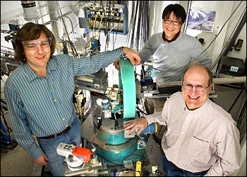 |
| Alexei Tkachenko, Htay Hlaing and Ben Ocko at an experimental end station at the NSLS. |
Abstract:
As part of the quest to form perfectly smooth single-molecule layers of materials for advanced energy, electronic, and medical devices, researchers at the U.S. Department of Energy's Brookhaven National Laboratory have discovered that the molecules in thin films remain frozen at a temperature where the bulk material is molten. Thin molecular films have a range of applications extending from organic solar cells to biosensors, and understanding the fundamental aspects of these films could lead to improved devices.
Expanding the Degrees of Surface Freezing: Molecular ordering phenomenon found at interface between complex liquids and solids
Upton, NY | Posted on March 30th, 2011The study, which appears in the April 1, 2011, edition of Physical Review Letters (now online at: link.aps.org/doi/10.1103/PhysRevLett.106.137801), is the first to directly observe "surface freezing" at the buried interface between bulk liquids and solid surfaces.
"In most materials, you expect that the surface will start to disorder and eventually melt at a temperature where the bulk remains solid," said Brookhaven physicist Ben Ocko, who collaborated on the research with scientists from the European Synchrotron Radiation Facility (ESRF), in France, and Bar-Ilan University, in Israel. "This is because the molecules on the outside are less confined than those packed in the deeper layers and much more able to move around. But surface freezing contradicts this basic idea. In surface freezing, the interfacial layers freeze before the bulk."
In the early 1990s, two independent teams (one at Brookhaven) made the first observation of surface freezing at the vapor interface of bulk alkanes, organic molecules similar to those in candle wax that contain only carbon and hydrogen atoms. Surface freezing has since been observed in a range of simple chain molecules and at various interfaces between them.
"The mechanics of surface freezing are still a mystery," said Bar Ilan scientist Moshe Deutsch. "It's puzzling why alkanes and their derivatives show this unusual effect, while virtually all other materials exhibit the opposite, surface melting, effect."
In the most recent study, the researchers discovered that surface freezing also occurs at the interface between a liquid and a solid surface. In a temperature-controlled environment at Brookhaven's National Synchrotron Light Source (NSLS, http://www.nsls.bnl.gov/) and the ESRF, the group made contact between a piece of highly polished sapphire and a puddle of liquid alkanol -- a long-chain alcohol. The researchers shot a beam of high-intensity x-rays through the interface and by measuring how the x-rays reflected off the sample, the group revealed that the alkanol molecules at the sapphire surface behave very differently from those in the bulk liquid.
According to ESRF scientist Diego Pontoni, "Surprisingly, the alkanol molecules form a perfect frozen monolayer at the sapphire interface at temperatures where the bulk is still liquid." At sufficiently high temperatures, about 30 degrees Celsius above the melting temperature of the bulk alkanol, the monolayer also melts.
The temperature range over which this frozen monolayer exists is about 10 times greater than what's observed at the liquid-vapor interfaces of similar materials. According to Alexei Tkachenko, a theoretical physicist who works at Brookhaven's Center for Functional Nanomaterials (CFN, www.bnl.gov/cfn/), "The temperature range of the surface-frozen layer and its temperature-dependent thickness can be described by a very simple model that we developed. What is remarkable is that the surface layer does not freeze abruptly as in the case of ice, or any other crystal. Rather, a smooth transition occurs over a temperature range of several degrees."
Said Ocko, "These films are better ordered and smoother than all other organic monolayer films created to date."
Moshe Deutsch added, "The results of this study and the theoretical framework which it provides may lead to new ideas on how to make defect-free, single molecule-thick films."
Funding for this work was provided by the U.S. Department of Energy's Office of Science and the U.S.-Israel Binational Science Foundation.
The Center for Functional Nanomaterials at Brookhaven National Laboratory is one of the five DOE Nanoscale Science Research Centers (NSRCs), premier national user facilities for interdisciplinary research at the nanoscale. Together the NSRCs comprise a suite of complementary facilities that provide researchers with state-of-the-art capabilities to fabricate, process, characterize and model nanoscale materials, and constitute the largest infrastructure investment of the National Nanotechnology Initiative. The NSRCs are located at DOE's Argonne, Brookhaven, Lawrence Berkeley, Oak Ridge and Sandia and Los Alamos national laboratories.
####
About Brookhaven National Laboratory
One of ten national laboratories overseen and primarily funded by the Office of Science of the U.S. Department of Energy (DOE), Brookhaven National Laboratory conducts research in the physical, biomedical, and environmental sciences, as well as in energy technologies and national security. Brookhaven Lab also builds and operates major scientific facilities available to university, industry and government researchers. Brookhaven is operated and managed for DOE's Office of Science by Brookhaven Science Associates, a limited-liability company founded by the Research Foundation of State University of New York on behalf of Stony Brook University, the largest academic user of Laboratory facilities, and Battelle, a nonprofit, applied science and technology organization.
Visit Brookhaven Lab's electronic newsroom for links, news archives, graphics, and more at www.bnl.gov/newsroom , or follow Brookhaven Lab on Twitter, twitter.com/BrookhavenLab .
For more information, please click here
Contacts:
Peter Genzer
(631) 344-3174
or
Karen McNulty Walsh
(631) 344-8350
Copyright © Brookhaven National Laboratory
If you have a comment, please Contact us.Issuers of news releases, not 7th Wave, Inc. or Nanotechnology Now, are solely responsible for the accuracy of the content.
Bookmark:


| Related News Press |
Physics
![]() Simulating magnetization in a Heisenberg quantum spin chain April 5th, 2024
Simulating magnetization in a Heisenberg quantum spin chain April 5th, 2024
![]() Nanoscale CL thermometry with lanthanide-doped heavy-metal oxide in TEM March 8th, 2024
Nanoscale CL thermometry with lanthanide-doped heavy-metal oxide in TEM March 8th, 2024
![]() Optically trapped quantum droplets of light can bind together to form macroscopic complexes March 8th, 2024
Optically trapped quantum droplets of light can bind together to form macroscopic complexes March 8th, 2024
![]() 'Sudden death' of quantum fluctuations defies current theories of superconductivity: Study challenges the conventional wisdom of superconducting quantum transitions January 12th, 2024
'Sudden death' of quantum fluctuations defies current theories of superconductivity: Study challenges the conventional wisdom of superconducting quantum transitions January 12th, 2024
News and information
![]() Simulating magnetization in a Heisenberg quantum spin chain April 5th, 2024
Simulating magnetization in a Heisenberg quantum spin chain April 5th, 2024
![]() NRL charters Navy�s quantum inertial navigation path to reduce drift April 5th, 2024
NRL charters Navy�s quantum inertial navigation path to reduce drift April 5th, 2024
![]() Discovery points path to flash-like memory for storing qubits: Rice find could hasten development of nonvolatile quantum memory April 5th, 2024
Discovery points path to flash-like memory for storing qubits: Rice find could hasten development of nonvolatile quantum memory April 5th, 2024
![]() Good as gold - improving infectious disease testing with gold nanoparticles April 5th, 2024
Good as gold - improving infectious disease testing with gold nanoparticles April 5th, 2024
Thin films
![]() Utilizing palladium for addressing contact issues of buried oxide thin film transistors April 5th, 2024
Utilizing palladium for addressing contact issues of buried oxide thin film transistors April 5th, 2024
Laboratories
![]() A battery�s hopping ions remember where they�ve been: Seen in atomic detail, the seemingly smooth flow of ions through a battery�s electrolyte is surprisingly complicated February 16th, 2024
A battery�s hopping ions remember where they�ve been: Seen in atomic detail, the seemingly smooth flow of ions through a battery�s electrolyte is surprisingly complicated February 16th, 2024
![]() NRL discovers two-dimensional waveguides February 16th, 2024
NRL discovers two-dimensional waveguides February 16th, 2024
Chip Technology
![]() Discovery points path to flash-like memory for storing qubits: Rice find could hasten development of nonvolatile quantum memory April 5th, 2024
Discovery points path to flash-like memory for storing qubits: Rice find could hasten development of nonvolatile quantum memory April 5th, 2024
![]() Utilizing palladium for addressing contact issues of buried oxide thin film transistors April 5th, 2024
Utilizing palladium for addressing contact issues of buried oxide thin film transistors April 5th, 2024
![]() HKUST researchers develop new integration technique for efficient coupling of III-V and silicon February 16th, 2024
HKUST researchers develop new integration technique for efficient coupling of III-V and silicon February 16th, 2024
Sensors
Nanoelectronics
![]() Interdisciplinary: Rice team tackles the future of semiconductors Multiferroics could be the key to ultralow-energy computing October 6th, 2023
Interdisciplinary: Rice team tackles the future of semiconductors Multiferroics could be the key to ultralow-energy computing October 6th, 2023
![]() Key element for a scalable quantum computer: Physicists from Forschungszentrum J�lich and RWTH Aachen University demonstrate electron transport on a quantum chip September 23rd, 2022
Key element for a scalable quantum computer: Physicists from Forschungszentrum J�lich and RWTH Aachen University demonstrate electron transport on a quantum chip September 23rd, 2022
![]() Reduced power consumption in semiconductor devices September 23rd, 2022
Reduced power consumption in semiconductor devices September 23rd, 2022
![]() Atomic level deposition to extend Moore�s law and beyond July 15th, 2022
Atomic level deposition to extend Moore�s law and beyond July 15th, 2022
Discoveries
![]() Chemical reactions can scramble quantum information as well as black holes April 5th, 2024
Chemical reactions can scramble quantum information as well as black holes April 5th, 2024
![]() New micromaterial releases nanoparticles that selectively destroy cancer cells April 5th, 2024
New micromaterial releases nanoparticles that selectively destroy cancer cells April 5th, 2024
![]() Utilizing palladium for addressing contact issues of buried oxide thin film transistors April 5th, 2024
Utilizing palladium for addressing contact issues of buried oxide thin film transistors April 5th, 2024
Announcements
![]() NRL charters Navy�s quantum inertial navigation path to reduce drift April 5th, 2024
NRL charters Navy�s quantum inertial navigation path to reduce drift April 5th, 2024
![]() Discovery points path to flash-like memory for storing qubits: Rice find could hasten development of nonvolatile quantum memory April 5th, 2024
Discovery points path to flash-like memory for storing qubits: Rice find could hasten development of nonvolatile quantum memory April 5th, 2024
Energy
![]() Development of zinc oxide nanopagoda array photoelectrode: photoelectrochemical water-splitting hydrogen production January 12th, 2024
Development of zinc oxide nanopagoda array photoelectrode: photoelectrochemical water-splitting hydrogen production January 12th, 2024
![]() Shedding light on unique conduction mechanisms in a new type of perovskite oxide November 17th, 2023
Shedding light on unique conduction mechanisms in a new type of perovskite oxide November 17th, 2023
![]() Inverted perovskite solar cell breaks 25% efficiency record: Researchers improve cell efficiency using a combination of molecules to address different November 17th, 2023
Inverted perovskite solar cell breaks 25% efficiency record: Researchers improve cell efficiency using a combination of molecules to address different November 17th, 2023
![]() The efficient perovskite cells with a structured anti-reflective layer � another step towards commercialization on a wider scale October 6th, 2023
The efficient perovskite cells with a structured anti-reflective layer � another step towards commercialization on a wider scale October 6th, 2023
Solar/Photovoltaic
![]() Development of zinc oxide nanopagoda array photoelectrode: photoelectrochemical water-splitting hydrogen production January 12th, 2024
Development of zinc oxide nanopagoda array photoelectrode: photoelectrochemical water-splitting hydrogen production January 12th, 2024
![]() Shedding light on unique conduction mechanisms in a new type of perovskite oxide November 17th, 2023
Shedding light on unique conduction mechanisms in a new type of perovskite oxide November 17th, 2023
![]() Inverted perovskite solar cell breaks 25% efficiency record: Researchers improve cell efficiency using a combination of molecules to address different November 17th, 2023
Inverted perovskite solar cell breaks 25% efficiency record: Researchers improve cell efficiency using a combination of molecules to address different November 17th, 2023
![]() Charged �molecular beasts� the basis for new compounds: Researchers at Leipzig University use �aggressive� fragments of molecular ions for chemical synthesis November 3rd, 2023
Charged �molecular beasts� the basis for new compounds: Researchers at Leipzig University use �aggressive� fragments of molecular ions for chemical synthesis November 3rd, 2023
|
|
||
|
|
||
| The latest news from around the world, FREE | ||
|
|
||
|
|
||
| Premium Products | ||
|
|
||
|
Only the news you want to read!
Learn More |
||
|
|
||
|
Full-service, expert consulting
Learn More |
||
|
|
||