Home > Press > New Technique Boosts High-Power Potential For Gallium Nitride Electronics
 |
| By implanting a buffer made of argon, researchers have created GaN devices that can handle 10 times as much power. |
Abstract:
Researchers at North Carolina State University have solved the problem, introducing a buffer that allows the GaN devices to handle 10 times greater power.
New Technique Boosts High-Power Potential For Gallium Nitride Electronics
Raleigh, NC | Posted on February 4th, 2011Gallium nitride (GaN) material holds promise for emerging high-power devices that are more energy efficient than existing technologies - but these GaN devices traditionally break down when exposed to high voltages. Now researchers at North Carolina State University have solved the problem, introducing a buffer that allows the GaN devices to handle 10 times greater power.
"For future renewable technologies, such as the smart grid or electric cars, we need high-power semiconductor devices," says Merve Ozbek, a Ph.D. student at NC State and author of a paper describing the research. "And power-handling capacity is important for the development of those devices."
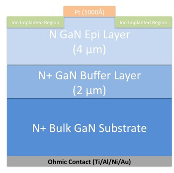
Previous research into developing high power GaN devices ran into obstacles, because large electric fields were created at specific points on the devices' edge when high voltages were applied - effectively destroying the devices. NC State researchers have addressed the problem by implanting a buffer made of the element argon at the edges of GaN devices. The buffer spreads out the electric field, allowing the device to handle much higher voltages.
The researchers tested the new technique on Schottky diodes - common electronic components - and found that the argon implant allowed the GaN diodes to handle almost seven times higher voltages. The diodes that did not have the argon implant broke down when exposed to approximately 250 volts. The diodes with the argon implant could handle up to 1,650 volts before breaking down.
"By improving the breakdown voltage from 250 volts to 1,650 volts, we can reduce the electrical resistance of these devices a hundredfold," says Dr. Jay Baliga, Distinguished University Professor of Electrical and Computer Engineering at NC State and co-author of the paper. "That reduction in resistance means that these devices can handle ten times as much power."
The paper, "Planar, Nearly Ideal Edge Termination Technique for GaN Devices," is forthcoming from IEEE's Electron Device Letters. The research was supported by NC State's Future Renewable Electric Energy Delivery and Management Systems Center, with funding from the National Science Foundation.
NC State's Department of Electrical and Computer Engineering is part of the university's College of Engineering.
Abstract
"Planar, Nearly Ideal Edge Termination Technique for GaN Devices"
Authors: A. Merve Ozbek, B. Jayant Baliga, North Carolina State University
Published: Forthcoming, Electron Device Letters
Abstract: In this paper, a simple edge termination is described which can be used to achieve nearly ideal parallel plane breakdown voltage for GaN devices. This technique involves implanting a neutral species on the edges of devices to form a high resistive amorphous layer. With this termination, formed by using argon implantation, the breakdown voltage of GaN Schottky barrier diodes were increased from 300V for unterminated diodes to 1650V after termination.
####
For more information, please click here
Contacts:
Matt Shipman
News Services
919.515.6386
Dr. Jay Baliga
919.515.6169
Copyright © North Carolina State University
If you have a comment, please Contact us.Issuers of news releases, not 7th Wave, Inc. or Nanotechnology Now, are solely responsible for the accuracy of the content.
Bookmark:


| Related News Press |
News and information
![]() Simulating magnetization in a Heisenberg quantum spin chain April 5th, 2024
Simulating magnetization in a Heisenberg quantum spin chain April 5th, 2024
![]() NRL charters Navy�s quantum inertial navigation path to reduce drift April 5th, 2024
NRL charters Navy�s quantum inertial navigation path to reduce drift April 5th, 2024
![]() Discovery points path to flash-like memory for storing qubits: Rice find could hasten development of nonvolatile quantum memory April 5th, 2024
Discovery points path to flash-like memory for storing qubits: Rice find could hasten development of nonvolatile quantum memory April 5th, 2024
Govt.-Legislation/Regulation/Funding/Policy
![]() NRL charters Navy�s quantum inertial navigation path to reduce drift April 5th, 2024
NRL charters Navy�s quantum inertial navigation path to reduce drift April 5th, 2024
![]() Discovery points path to flash-like memory for storing qubits: Rice find could hasten development of nonvolatile quantum memory April 5th, 2024
Discovery points path to flash-like memory for storing qubits: Rice find could hasten development of nonvolatile quantum memory April 5th, 2024
![]() Chemical reactions can scramble quantum information as well as black holes April 5th, 2024
Chemical reactions can scramble quantum information as well as black holes April 5th, 2024
Possible Futures
![]() Discovery points path to flash-like memory for storing qubits: Rice find could hasten development of nonvolatile quantum memory April 5th, 2024
Discovery points path to flash-like memory for storing qubits: Rice find could hasten development of nonvolatile quantum memory April 5th, 2024
![]() With VECSELs towards the quantum internet Fraunhofer: IAF achieves record output power with VECSEL for quantum frequency converters April 5th, 2024
With VECSELs towards the quantum internet Fraunhofer: IAF achieves record output power with VECSEL for quantum frequency converters April 5th, 2024
Academic/Education
![]() Rice University launches Rice Synthetic Biology Institute to improve lives January 12th, 2024
Rice University launches Rice Synthetic Biology Institute to improve lives January 12th, 2024
![]() Multi-institution, $4.6 million NSF grant to fund nanotechnology training September 9th, 2022
Multi-institution, $4.6 million NSF grant to fund nanotechnology training September 9th, 2022
Chip Technology
![]() Discovery points path to flash-like memory for storing qubits: Rice find could hasten development of nonvolatile quantum memory April 5th, 2024
Discovery points path to flash-like memory for storing qubits: Rice find could hasten development of nonvolatile quantum memory April 5th, 2024
![]() Utilizing palladium for addressing contact issues of buried oxide thin film transistors April 5th, 2024
Utilizing palladium for addressing contact issues of buried oxide thin film transistors April 5th, 2024
![]() HKUST researchers develop new integration technique for efficient coupling of III-V and silicon February 16th, 2024
HKUST researchers develop new integration technique for efficient coupling of III-V and silicon February 16th, 2024
Nanoelectronics
![]() Interdisciplinary: Rice team tackles the future of semiconductors Multiferroics could be the key to ultralow-energy computing October 6th, 2023
Interdisciplinary: Rice team tackles the future of semiconductors Multiferroics could be the key to ultralow-energy computing October 6th, 2023
![]() Key element for a scalable quantum computer: Physicists from Forschungszentrum J�lich and RWTH Aachen University demonstrate electron transport on a quantum chip September 23rd, 2022
Key element for a scalable quantum computer: Physicists from Forschungszentrum J�lich and RWTH Aachen University demonstrate electron transport on a quantum chip September 23rd, 2022
![]() Reduced power consumption in semiconductor devices September 23rd, 2022
Reduced power consumption in semiconductor devices September 23rd, 2022
![]() Atomic level deposition to extend Moore�s law and beyond July 15th, 2022
Atomic level deposition to extend Moore�s law and beyond July 15th, 2022
Announcements
![]() NRL charters Navy�s quantum inertial navigation path to reduce drift April 5th, 2024
NRL charters Navy�s quantum inertial navigation path to reduce drift April 5th, 2024
![]() Discovery points path to flash-like memory for storing qubits: Rice find could hasten development of nonvolatile quantum memory April 5th, 2024
Discovery points path to flash-like memory for storing qubits: Rice find could hasten development of nonvolatile quantum memory April 5th, 2024
|
|
||
|
|
||
| The latest news from around the world, FREE | ||
|
|
||
|
|
||
| Premium Products | ||
|
|
||
|
Only the news you want to read!
Learn More |
||
|
|
||
|
Full-service, expert consulting
Learn More |
||
|
|
||