Home > Press > New Transistor for Plastic Electronics Exhibits the Best of Both Worlds
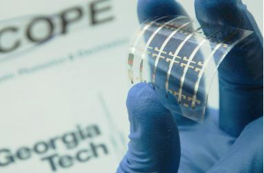 |
| Top-Gate Organic Field-Effect Transistor with Bilayer Gate Insulator. Bernard Kippelen and his research team at the Center for Organic Photonics and Electronics have demonstrated a new transistor for use on flexible plastic electronics, known as a top-gate organic field-effect transistor with a bilayer gate insulator. The transistor's properties give it incredible stability while exhibiting good performance. Photo credit: Canek Fuentes-Herandez/Georgia Tech |
Abstract:
In the quest to develop flexible plastic electronics, one of the stumbling blocks has been creating transistors with enough stability for them to function in a variety of environments while still maintaining the current needed to power the devices.
New Transistor for Plastic Electronics Exhibits the Best of Both Worlds
Atlanta, GA | Posted on January 28th, 2011Online in the journal Advanced Materials, researchers from the Georgia Institute of Technology describe a new method of combining top-gate organic field-effect transistors with a bilayer gate insulator. This allows the transistor to perform with incredible stability while exhibiting good current performance. In addition, the transistor can be mass produced in a regular atmosphere and can be created using lower temperatures, making it compatible with the plastic devices it will power.
The research team used an existing semiconductor and changed the gate dielectric because transistor performance depends not only on the semiconductor itself, but also on the interface between the semiconductor and the gate dielectric.
"Rather than using a single dielectric material, as many have done in the past, we developed a bilayer gate dielectric," said Bernard Kippelen, director of the Center for Organic Photonics and Electronics and professor in Georgia Tech's School of Electrical and Computer Engineering.
The bilayer dielectric is made of a fluorinated polymer known as CYTOP and a high-k metal-oxide layer created by atomic layer deposition. Used alone, each substance has its benefits and its drawbacks.
CYTOP is known to form few defects at the interface of the organic semiconductor, but it also has a very low dielectric constant, which requires an increase in drive voltage. The high-k metal-oxide uses low voltage, but doesn't have good stability because of a high number of defects on the interface.
So, Kippelen and his team wondered what would happen if they combined the two substances in a bilayer. Would the drawbacks cancel each other out?
"When we started to do the test experiments, the results were stunning. We were expecting good stability, but not to the point of having no degradation in mobility for more than a year," said Kippelen.
The team performed a battery of tests to see just how stable the bilayer was. They cycled the transistors 20,000 times. There was no degradation. They tested it under a continuous bias stress where they ran the highest possible current through it. There was no degradation. They even stuck it in a plasma chamber for five minutes. There was still no degradation.
The only time they saw any degradation was when they dropped it into acetone for an hour. There was some degradation, but the transistor was still operational.
No one was more surprised than Kippelen.
"I had always questioned the concept of having air-stable field-effect transistors, because I thought you would always have to combine the transistors with some barrier coating to protect them from oxygen and moisture. We've proven ourselves wrong through this work," said Kippelen.
"By having the bilayer gate insulator we have two different degradation mechanisms that happen at the same time, but the effects are such that they compensate for one another," explains Kippelen. "So if you use one it leads to a decrease of the current, if you use the other it leads to a shift of the thereshold voltage and over time to an increase of the current. But if you combine them, their effects cancel out."
"This is an elegant way of solving the problem. So, rather than trying to remove each effect, we took two processes that complement one another and as a result you have a transistor that's rock stable."
The transistor conducts current and runs at a voltage comparable to amorphous silicon, the current industry standard used on glass substrates, but can be manufactured at temperatures below 150�C, in line with the capabilities of plastic substrates. It can also be created in a regular atmosphere, making it easier to fabricate than other transistors.
Applications for these transistors include smart bandages, RFID tags, plastic solar cells, light emitters for smart cards - virtually any application where stable power and a flexible surface are needed.
In this paper the tests were performed on glass substrates. Next, the team plans on demonstrating the transistors on flexible plastic substrates. Then they will test the ability to manufacture the bilayer transistors with ink jet printing technologies.
Kippelen's research team was comprised of Do Kyung Hwang, Canek Fuentes-Hernandez, Jungbae Kim, William J. Postcavage Jr. and Sung-Jin Kim.
The research was supported by Solvay, the Office of Naval Research and the National Science Foundation.
####
About Georgia Institute of Technology
The Georgia Institute of Technology is one of the world's premier research universities. Ranked seventh among U.S. News & World Report's top public universities and the eighth best engineering and information technology university in the world by Shanghai Jiao Tong University's Academic Ranking of World Universities, Georgia Tech�s more than 20,000 students are enrolled in its Colleges of Architecture, Computing, Engineering, Liberal Arts, Management and Sciences. Tech is among the nation's top producers of women and minority engineers. The Institute offers research opportunities to both undergraduate and graduate students and is home to more than 100 interdisciplinary units plus the Georgia Tech Research Institute.
For more information, please click here
Contacts:
David Terraso
Communications and Marketing
404-385-2966
Copyright © Georgia Institute of Technology
If you have a comment, please Contact us.Issuers of news releases, not 7th Wave, Inc. or Nanotechnology Now, are solely responsible for the accuracy of the content.
Bookmark:


| Related News Press |
News and information
![]() Researchers develop molecular qubits that communicate at telecom frequencies October 3rd, 2025
Researchers develop molecular qubits that communicate at telecom frequencies October 3rd, 2025
![]() Next-generation quantum communication October 3rd, 2025
Next-generation quantum communication October 3rd, 2025
![]() "Nanoreactor" cage uses visible light for catalytic and ultra-selective cross-cycloadditions October 3rd, 2025
"Nanoreactor" cage uses visible light for catalytic and ultra-selective cross-cycloadditions October 3rd, 2025
Govt.-Legislation/Regulation/Funding/Policy
![]() New imaging approach transforms study of bacterial biofilms August 8th, 2025
New imaging approach transforms study of bacterial biofilms August 8th, 2025
![]() Electrifying results shed light on graphene foam as a potential material for lab grown cartilage June 6th, 2025
Electrifying results shed light on graphene foam as a potential material for lab grown cartilage June 6th, 2025
![]() Institute for Nanoscience hosts annual proposal planning meeting May 16th, 2025
Institute for Nanoscience hosts annual proposal planning meeting May 16th, 2025
Possible Futures
![]() Spinel-type sulfide semiconductors to operate the next-generation LEDs and solar cells For solar-cell absorbers and green-LED source October 3rd, 2025
Spinel-type sulfide semiconductors to operate the next-generation LEDs and solar cells For solar-cell absorbers and green-LED source October 3rd, 2025
Academic/Education
![]() Rice University launches Rice Synthetic Biology Institute to improve lives January 12th, 2024
Rice University launches Rice Synthetic Biology Institute to improve lives January 12th, 2024
![]() Multi-institution, $4.6 million NSF grant to fund nanotechnology training September 9th, 2022
Multi-institution, $4.6 million NSF grant to fund nanotechnology training September 9th, 2022
Chip Technology
![]() Lab to industry: InSe wafer-scale breakthrough for future electronics August 8th, 2025
Lab to industry: InSe wafer-scale breakthrough for future electronics August 8th, 2025
![]() A 1960s idea inspires NBI researchers to study hitherto inaccessible quantum states June 6th, 2025
A 1960s idea inspires NBI researchers to study hitherto inaccessible quantum states June 6th, 2025
![]() Programmable electron-induced color router array May 14th, 2025
Programmable electron-induced color router array May 14th, 2025
Nanomedicine
![]() New molecular technology targets tumors and simultaneously silences two �undruggable� cancer genes August 8th, 2025
New molecular technology targets tumors and simultaneously silences two �undruggable� cancer genes August 8th, 2025
![]() New imaging approach transforms study of bacterial biofilms August 8th, 2025
New imaging approach transforms study of bacterial biofilms August 8th, 2025
![]() Cambridge chemists discover simple way to build bigger molecules � one carbon at a time June 6th, 2025
Cambridge chemists discover simple way to build bigger molecules � one carbon at a time June 6th, 2025
![]() Electrifying results shed light on graphene foam as a potential material for lab grown cartilage June 6th, 2025
Electrifying results shed light on graphene foam as a potential material for lab grown cartilage June 6th, 2025
Nanoelectronics
![]() Lab to industry: InSe wafer-scale breakthrough for future electronics August 8th, 2025
Lab to industry: InSe wafer-scale breakthrough for future electronics August 8th, 2025
![]() Interdisciplinary: Rice team tackles the future of semiconductors Multiferroics could be the key to ultralow-energy computing October 6th, 2023
Interdisciplinary: Rice team tackles the future of semiconductors Multiferroics could be the key to ultralow-energy computing October 6th, 2023
![]() Key element for a scalable quantum computer: Physicists from Forschungszentrum J�lich and RWTH Aachen University demonstrate electron transport on a quantum chip September 23rd, 2022
Key element for a scalable quantum computer: Physicists from Forschungszentrum J�lich and RWTH Aachen University demonstrate electron transport on a quantum chip September 23rd, 2022
![]() Reduced power consumption in semiconductor devices September 23rd, 2022
Reduced power consumption in semiconductor devices September 23rd, 2022
Announcements
![]() Rice membrane extracts lithium from brines with greater speed, less waste October 3rd, 2025
Rice membrane extracts lithium from brines with greater speed, less waste October 3rd, 2025
![]() Researchers develop molecular qubits that communicate at telecom frequencies October 3rd, 2025
Researchers develop molecular qubits that communicate at telecom frequencies October 3rd, 2025
![]() Next-generation quantum communication October 3rd, 2025
Next-generation quantum communication October 3rd, 2025
![]() "Nanoreactor" cage uses visible light for catalytic and ultra-selective cross-cycloadditions October 3rd, 2025
"Nanoreactor" cage uses visible light for catalytic and ultra-selective cross-cycloadditions October 3rd, 2025
Nanobiotechnology
![]() New molecular technology targets tumors and simultaneously silences two �undruggable� cancer genes August 8th, 2025
New molecular technology targets tumors and simultaneously silences two �undruggable� cancer genes August 8th, 2025
![]() New imaging approach transforms study of bacterial biofilms August 8th, 2025
New imaging approach transforms study of bacterial biofilms August 8th, 2025
![]() Ben-Gurion University of the Negev researchers several steps closer to harnessing patient's own T-cells to fight off cancer June 6th, 2025
Ben-Gurion University of the Negev researchers several steps closer to harnessing patient's own T-cells to fight off cancer June 6th, 2025
![]() Electrifying results shed light on graphene foam as a potential material for lab grown cartilage June 6th, 2025
Electrifying results shed light on graphene foam as a potential material for lab grown cartilage June 6th, 2025
Solar/Photovoltaic
![]() Spinel-type sulfide semiconductors to operate the next-generation LEDs and solar cells For solar-cell absorbers and green-LED source October 3rd, 2025
Spinel-type sulfide semiconductors to operate the next-generation LEDs and solar cells For solar-cell absorbers and green-LED source October 3rd, 2025
![]() KAIST researchers introduce new and improved, next-generation perovskite solar cell November 8th, 2024
KAIST researchers introduce new and improved, next-generation perovskite solar cell November 8th, 2024
![]() Groundbreaking precision in single-molecule optoelectronics August 16th, 2024
Groundbreaking precision in single-molecule optoelectronics August 16th, 2024
![]() Development of zinc oxide nanopagoda array photoelectrode: photoelectrochemical water-splitting hydrogen production January 12th, 2024
Development of zinc oxide nanopagoda array photoelectrode: photoelectrochemical water-splitting hydrogen production January 12th, 2024
RFID
![]() Nanowire 'inks' enable paper-based printable electronics: Highly conductive films make functional circuits without adding high heat January 4th, 2017
Nanowire 'inks' enable paper-based printable electronics: Highly conductive films make functional circuits without adding high heat January 4th, 2017
![]() Conformal transfer of graphene for reproducible device fabrication August 11th, 2015
Conformal transfer of graphene for reproducible device fabrication August 11th, 2015
|
|
||
|
|
||
| The latest news from around the world, FREE | ||
|
|
||
|
|
||
| Premium Products | ||
|
|
||
|
Only the news you want to read!
Learn More |
||
|
|
||
|
Full-service, expert consulting
Learn More |
||
|
|
||