Home > Press > Graphene grains make atomic patchwork quilts
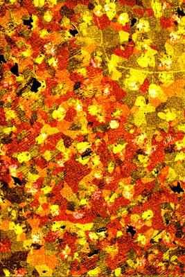 |
| A false-color microscopy image overlay depicting the shapes and lattice orientations of several grains in graphene. Credit: Muller Lab |
Abstract:
A quick look at new Cornell research hints at colorful patchwork quilts, but they are actually pictures of graphene -- one atom-thick sheets of carbon stitched together at tilted interfaces. Researchers have unveiled striking, atomic-resolution details of what graphene "quilts" look like at the boundaries between patches, and have uncovered key insights into graphene's electrical and mechanical properties.
By Anne Ju
Graphene grains make atomic patchwork quilts
Ithaca, NY | Posted on January 5th, 2011The multidisciplinary Cornell collaboration, publishing online Jan. 5 in the journal Nature, focuses on graphene -- a one atom-thick sheet of carbon atoms bonded in a crystal lattice like a honeycomb or chicken wire -- because of its electrical properties and potential to improve anything from solar cells to cell phone screens. But it doesn't grow in perfect sheets; rather, it develops in pieces that resemble patchwork quilts, where the honeycomb lattice meets up imperfectly and creates five- or seven-member carbon rings, rather than the perfect six. Where these "patches" meet are called grain boundaries, and scientists had wondered whether these boundaries would allow the special properties of a perfect graphene crystal to transfer to the much larger quilt-like structures.
To study the material, the researchers grew graphene membranes on a copper substrate (a method devised by another group) but then conceived a novel way to peel them off as free-standing, atom-thick films. Then, with diffraction imaging electron microscopy, they imaged the graphene by seeing how electrons bounced off at certain angles, and using a color to represent that angle. By overlaying different colors according to how the electrons bounced, they created an easy, efficient method of imaging the graphene grain boundaries according to their orientation. And as a bonus, their pictures took an artistic turn, reminding the scientists of patchwork quilts.
"You don't want to look at the whole quilt by counting each thread," said David Muller, professor of applied and engineering physics and co-director of the Kavli Institute at Cornell for Nanoscale Science, who conducted the work with Paul McEuen, professor of physics and director of the Kavli Institute; and Kavli member Jiwoong Park, assistant professor of chemistry and chemical biology. "You want to stand back and see what it looks like on the bed. And so we developed a method that filters out the crystal information in a way that you don't have to count every atom."
This new method could apply to other two-dimensional materials and sheds new light on the previously mysterious way that graphene was stitched together at grain boundaries.
Further analysis revealed that growing larger grains (bigger patches) didn't improve the electrical conductivity of the graphene, as was previously thought by materials scientists. Rather, it is impurities that sneak into the sheets that make the electrical properties fluctuate. This insight will lead scientists closer to the best ways to grow and use graphene.
The work was supported by the National Science Foundation through the Cornell Center for Materials Research and the Nanoscale Science and Engineering Initiative. The paper's other contributors were: Pinshane Huang (applied and engineering physics), Carlos Ruiz-Vargas (applied and engineering physics), Arend van der Zande (physics), William Whitney (physics), Mark Levendorf (chemistry), Joshua Kevek (Oregon State), Shivank Garg (chemistry), Jonathan Alden (applied and engineering physics), Caleb Hustedt (Brigham Young University) and Ye Zhu (applied and engineering physics).
####
For more information, please click here
Contacts:
Media Contact:
Blaine Friedlander
(607) 254-8093
Cornell Chronicle:
Anne Ju
(607) 255-9735
Copyright © Cornell University
If you have a comment, please Contact us.Issuers of news releases, not 7th Wave, Inc. or Nanotechnology Now, are solely responsible for the accuracy of the content.
Bookmark:


| Related News Press |
News and information
![]() Simulating magnetization in a Heisenberg quantum spin chain April 5th, 2024
Simulating magnetization in a Heisenberg quantum spin chain April 5th, 2024
![]() NRL charters Navy�s quantum inertial navigation path to reduce drift April 5th, 2024
NRL charters Navy�s quantum inertial navigation path to reduce drift April 5th, 2024
![]() Discovery points path to flash-like memory for storing qubits: Rice find could hasten development of nonvolatile quantum memory April 5th, 2024
Discovery points path to flash-like memory for storing qubits: Rice find could hasten development of nonvolatile quantum memory April 5th, 2024
![]() Good as gold - improving infectious disease testing with gold nanoparticles April 5th, 2024
Good as gold - improving infectious disease testing with gold nanoparticles April 5th, 2024
Display technology/LEDs/SS Lighting/OLEDs
![]() Utilizing palladium for addressing contact issues of buried oxide thin film transistors April 5th, 2024
Utilizing palladium for addressing contact issues of buried oxide thin film transistors April 5th, 2024
![]() Light guide plate based on perovskite nanocomposites November 3rd, 2023
Light guide plate based on perovskite nanocomposites November 3rd, 2023
![]() Simple ballpoint pen can write custom LEDs August 11th, 2023
Simple ballpoint pen can write custom LEDs August 11th, 2023
Govt.-Legislation/Regulation/Funding/Policy
![]() NRL charters Navy�s quantum inertial navigation path to reduce drift April 5th, 2024
NRL charters Navy�s quantum inertial navigation path to reduce drift April 5th, 2024
![]() Discovery points path to flash-like memory for storing qubits: Rice find could hasten development of nonvolatile quantum memory April 5th, 2024
Discovery points path to flash-like memory for storing qubits: Rice find could hasten development of nonvolatile quantum memory April 5th, 2024
![]() Chemical reactions can scramble quantum information as well as black holes April 5th, 2024
Chemical reactions can scramble quantum information as well as black holes April 5th, 2024
Possible Futures
![]() Discovery points path to flash-like memory for storing qubits: Rice find could hasten development of nonvolatile quantum memory April 5th, 2024
Discovery points path to flash-like memory for storing qubits: Rice find could hasten development of nonvolatile quantum memory April 5th, 2024
![]() With VECSELs towards the quantum internet Fraunhofer: IAF achieves record output power with VECSEL for quantum frequency converters April 5th, 2024
With VECSELs towards the quantum internet Fraunhofer: IAF achieves record output power with VECSEL for quantum frequency converters April 5th, 2024
Academic/Education
![]() Rice University launches Rice Synthetic Biology Institute to improve lives January 12th, 2024
Rice University launches Rice Synthetic Biology Institute to improve lives January 12th, 2024
![]() Multi-institution, $4.6 million NSF grant to fund nanotechnology training September 9th, 2022
Multi-institution, $4.6 million NSF grant to fund nanotechnology training September 9th, 2022
Nanotubes/Buckyballs/Fullerenes/Nanorods/Nanostrings
![]() Tests find no free-standing nanotubes released from tire tread wear September 8th, 2023
Tests find no free-standing nanotubes released from tire tread wear September 8th, 2023
![]() Detection of bacteria and viruses with fluorescent nanotubes July 21st, 2023
Detection of bacteria and viruses with fluorescent nanotubes July 21st, 2023
Announcements
![]() NRL charters Navy�s quantum inertial navigation path to reduce drift April 5th, 2024
NRL charters Navy�s quantum inertial navigation path to reduce drift April 5th, 2024
![]() Discovery points path to flash-like memory for storing qubits: Rice find could hasten development of nonvolatile quantum memory April 5th, 2024
Discovery points path to flash-like memory for storing qubits: Rice find could hasten development of nonvolatile quantum memory April 5th, 2024
Solar/Photovoltaic
![]() Development of zinc oxide nanopagoda array photoelectrode: photoelectrochemical water-splitting hydrogen production January 12th, 2024
Development of zinc oxide nanopagoda array photoelectrode: photoelectrochemical water-splitting hydrogen production January 12th, 2024
![]() Shedding light on unique conduction mechanisms in a new type of perovskite oxide November 17th, 2023
Shedding light on unique conduction mechanisms in a new type of perovskite oxide November 17th, 2023
![]() Inverted perovskite solar cell breaks 25% efficiency record: Researchers improve cell efficiency using a combination of molecules to address different November 17th, 2023
Inverted perovskite solar cell breaks 25% efficiency record: Researchers improve cell efficiency using a combination of molecules to address different November 17th, 2023
![]() Charged �molecular beasts� the basis for new compounds: Researchers at Leipzig University use �aggressive� fragments of molecular ions for chemical synthesis November 3rd, 2023
Charged �molecular beasts� the basis for new compounds: Researchers at Leipzig University use �aggressive� fragments of molecular ions for chemical synthesis November 3rd, 2023
|
|
||
|
|
||
| The latest news from around the world, FREE | ||
|
|
||
|
|
||
| Premium Products | ||
|
|
||
|
Only the news you want to read!
Learn More |
||
|
|
||
|
Full-service, expert consulting
Learn More |
||
|
|
||