Home > Press > Hydrogen and inert species improve solid phase epitaxy of Ge on Si
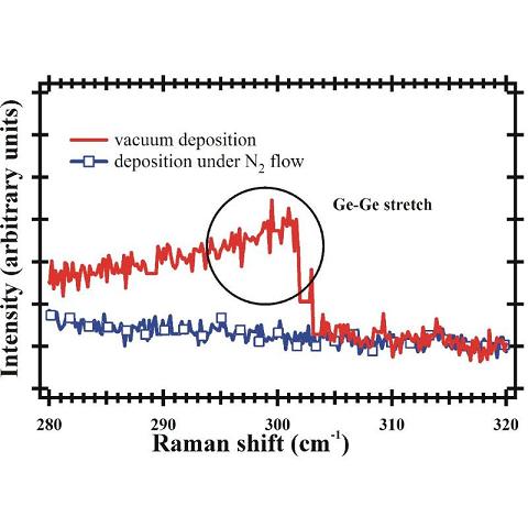 |
| (Color online) Comparison of Raman measurements of Ge layers deposited in vacuum (red, solid line) and deposited under N2 flux (blue, solid line with squares). For the vacuum deposited Ge layer, Ge�Ge stretch is observed, indicating the presence of structural ordering in the film. For the layer deposited under N2 flux no Ge�Ge stretch is visible, indicating complete disordering. |
Abstract:
Imec has shown that the presence of hydrogen and/or inert species during Ge deposition significantly improves the quality of the Ge layers grown on Si by solid phase epitaxy (SPE). The resulting layers have excellent crystalline quality and low surface roughness, making SPE a valuable alternative for conventional heteroepitaxy which is performed typically at much higher temperatures. High-quality Ge layers on Si are needed to explore the potential of Ge MOS devices for high-performance applications, or for extending conventional Si electronics.
Hydrogen and inert species improve solid phase epitaxy of Ge on Si
The Netherlands | Posted on April 21st, 2010Imec has demonstrated that the presence of atomic hydrogen during Ge deposition at low temperatures favors the formation of smooth and high-quality Ge layers on Si by SPE. A similar observation is made when molecular hydrogen, molecular nitrogen or chemical inert atoms or molecules are added during deposition. This results in high-quality single-crystalline Ge layers with surface roughness of only 0.4nm root mean square. In absence of these species, Ge layers grown by SPE exhibit low crystalline quality. The availability of high-quality thin Ge layers on Si is indispensible for the research on Ge and Ge/III-V devices. Ge on Si can potentially replace Si CMOS for high-performance applications and extends conventional Si electronics for e.g. optoelectronic applications.
In case of SPE, an amorphous layer is deposited on a crystalline substrate using methods such as (plasma enhanced) chemical vapor deposition ((PE)CVD) or ultrahigh vacuum (UHV) deposition. Subsequent annealing of the structure initiates crystallization at the interface, which continues towards the surface. In this way, an epitaxial layer can be formed on the substrate. SPE allows straightforward deposition of Ge on Si. Conventional heteroepitaxial growth on the contrary requires additional steps in order to reduce surface roughness.
Typically, PECVD using germane (GeH4) molecules is used to deposit the initial amorphous Ge layer. In this case, atomic hydrogen is inherently present and can influence the crystallization process in many ways. Imec's research shows that atomic hydrogen plays an important role during Ge deposition as it lowers the surface mobility of adsorbed Ge atoms and consequently increases the disorder of the deposited layer. Such a disordered layer is highly beneficial for SPE where crystallization has to start at the interface before it starts in the bulk. Atomic hydrogen is also incorporated into the growing layer, but it does not affect the crystallization process. A similar explanation can be given when fluxes of H2, N2 or chemical inert species are added during deposition by UHV. They also reduce the surface mobility and thereby the structural ordering of the Ge layers. In contrast to atomic hydrogen, these atoms are not incorporated into the growing film. The Ge deposition is performed at low temperatures (typically 150�C), subsequent crystallization is done by thermal annealing at 600�C in an N2 atmosphere for one minute. Annealing temperatures as low as 400�C can be applied. The low temperatures present an important advantage with respect to conventional heteroepitaxy, which is typically performed at much higher temperatures.
Detailed results of this study have been published by R.R. Lieten et al in Applied Physics Letters 94, 2009, �Solid phase epitaxy of amorphous Ge on Si in N2 atmosphere' and in Applied Physics Letters 96, 2010, �Hydrogen and inert species in solid phase epitaxy'.
####
About imec
Imec is Europe�s largest independent research center in nanoelectronics and nano-technology. Its staff of more than 1,750 people includes over 550 industrial residents and guest researchers. Imec�s research is applied in better healthcare, smart electronics, sustainable energy, and safer transport.
For more information, please click here
Copyright © imec
If you have a comment, please Contact us.Issuers of news releases, not 7th Wave, Inc. or Nanotechnology Now, are solely responsible for the accuracy of the content.
Bookmark:


| Related News Press |
News and information
![]() Simulating magnetization in a Heisenberg quantum spin chain April 5th, 2024
Simulating magnetization in a Heisenberg quantum spin chain April 5th, 2024
![]() NRL charters Navy�s quantum inertial navigation path to reduce drift April 5th, 2024
NRL charters Navy�s quantum inertial navigation path to reduce drift April 5th, 2024
![]() Discovery points path to flash-like memory for storing qubits: Rice find could hasten development of nonvolatile quantum memory April 5th, 2024
Discovery points path to flash-like memory for storing qubits: Rice find could hasten development of nonvolatile quantum memory April 5th, 2024
Possible Futures
![]() Discovery points path to flash-like memory for storing qubits: Rice find could hasten development of nonvolatile quantum memory April 5th, 2024
Discovery points path to flash-like memory for storing qubits: Rice find could hasten development of nonvolatile quantum memory April 5th, 2024
![]() With VECSELs towards the quantum internet Fraunhofer: IAF achieves record output power with VECSEL for quantum frequency converters April 5th, 2024
With VECSELs towards the quantum internet Fraunhofer: IAF achieves record output power with VECSEL for quantum frequency converters April 5th, 2024
Chip Technology
![]() Discovery points path to flash-like memory for storing qubits: Rice find could hasten development of nonvolatile quantum memory April 5th, 2024
Discovery points path to flash-like memory for storing qubits: Rice find could hasten development of nonvolatile quantum memory April 5th, 2024
![]() Utilizing palladium for addressing contact issues of buried oxide thin film transistors April 5th, 2024
Utilizing palladium for addressing contact issues of buried oxide thin film transistors April 5th, 2024
![]() HKUST researchers develop new integration technique for efficient coupling of III-V and silicon February 16th, 2024
HKUST researchers develop new integration technique for efficient coupling of III-V and silicon February 16th, 2024
Nanoelectronics
![]() Interdisciplinary: Rice team tackles the future of semiconductors Multiferroics could be the key to ultralow-energy computing October 6th, 2023
Interdisciplinary: Rice team tackles the future of semiconductors Multiferroics could be the key to ultralow-energy computing October 6th, 2023
![]() Key element for a scalable quantum computer: Physicists from Forschungszentrum J�lich and RWTH Aachen University demonstrate electron transport on a quantum chip September 23rd, 2022
Key element for a scalable quantum computer: Physicists from Forschungszentrum J�lich and RWTH Aachen University demonstrate electron transport on a quantum chip September 23rd, 2022
![]() Reduced power consumption in semiconductor devices September 23rd, 2022
Reduced power consumption in semiconductor devices September 23rd, 2022
![]() Atomic level deposition to extend Moore�s law and beyond July 15th, 2022
Atomic level deposition to extend Moore�s law and beyond July 15th, 2022
Announcements
![]() NRL charters Navy�s quantum inertial navigation path to reduce drift April 5th, 2024
NRL charters Navy�s quantum inertial navigation path to reduce drift April 5th, 2024
![]() Discovery points path to flash-like memory for storing qubits: Rice find could hasten development of nonvolatile quantum memory April 5th, 2024
Discovery points path to flash-like memory for storing qubits: Rice find could hasten development of nonvolatile quantum memory April 5th, 2024
Photonics/Optics/Lasers
![]() With VECSELs towards the quantum internet Fraunhofer: IAF achieves record output power with VECSEL for quantum frequency converters April 5th, 2024
With VECSELs towards the quantum internet Fraunhofer: IAF achieves record output power with VECSEL for quantum frequency converters April 5th, 2024
![]() Nanoscale CL thermometry with lanthanide-doped heavy-metal oxide in TEM March 8th, 2024
Nanoscale CL thermometry with lanthanide-doped heavy-metal oxide in TEM March 8th, 2024
![]() Optically trapped quantum droplets of light can bind together to form macroscopic complexes March 8th, 2024
Optically trapped quantum droplets of light can bind together to form macroscopic complexes March 8th, 2024
![]() HKUST researchers develop new integration technique for efficient coupling of III-V and silicon February 16th, 2024
HKUST researchers develop new integration technique for efficient coupling of III-V and silicon February 16th, 2024
|
|
||
|
|
||
| The latest news from around the world, FREE | ||
|
|
||
|
|
||
| Premium Products | ||
|
|
||
|
Only the news you want to read!
Learn More |
||
|
|
||
|
Full-service, expert consulting
Learn More |
||
|
|
||