Home > Press > The world's first junctionless nanowire transistor
 |
| Junctionless nanowire transistor successfully designed, simulated, fabricated and tested at Tyndall National Institute |
Abstract:
Tyndall breakthrough to revolutionise microchip manufacturing
The world's first junctionless nanowire transistor
Ireland | Posted on February 22nd, 2010A team of scientists at the Tyndall National Institute have designed and fabricated the world s first junctionless transistor that could revolutionise microchip manufacturing in the semiconductor industry. Prof. Jean-Pierre Colinge's breakthrough on the microchip transistor was published today in Nature Nanotechnology, one of the most prestigious scientific research publications.
The transistor is the fundamental building block in all electronic devices. Since the early seventies the number of transistors in a silicon chip has grown from a few hundred to over two billion transistors on a single chip today. The exponential increase in demand for feature packed electronic devices is driving the semiconductor industry to produce chips that need to be smaller, more energy efficient and more cost effective than ever before. As a consequence transistors are becoming so small that conventional transistor architectures, used since the seventies, can no longer be used.
"We have designed and fabricated the world's first junctionless transistor that significantly reduces power consumption and greatly simplifies the fabrication process of silicon chips," declared Tyndall's Professor Jean-Pierre Colinge.
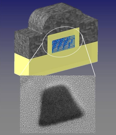
Current technologies require fabrication processes that are both complex and costly. All existing transistors are based on junctions. A junction is formed when two pieces of silicon with different polarities are placed side by side. Controlling the junction allows the current in the device to be turned on and off and it is the precise fabrication of this junction that determines the characteristics and quality of the transistor and is a major factor in the cost of production. Tyndall National Institute s ground breaking junctionless transistor doesn't require a junction. "The current flows in a very thin silicon wire and the flow of current is perfectly controlled by a `wedding ring` structure that electrically squeezes the silicon wire in the same way that you might stop the flow of water in a hose by squeezing it. These structures are easy to fabricate even on a miniature scale which leads to the major breakthrough in potential cost reduction," explained Professor Colinge.
Another key challenge for the semiconductor industry is reducing the power consumption of microchips. Minimising current leakage is one of the main challenges in today's complex transistors. "The Tyndall junctionless devices have near ideal electrical properties and behave like the most perfect transistors. Moreover, they have the potential of operating faster and using less energy than the conventional transistors used in today s microprocessors," said Professor Colinge.
He went on to say that the junctionless transistor resembles in a way the first ideal transistor structure, proposed in 1925. But to-date, no-one had been able to fabricate it. He attributed the successful fabrication at Tyndall to the skill and expertise of researchers who were able to fabricate silicon nanowire with a diameter of a few dozen atoms using electron-beam writing techniques and expertise available at Tyndall.
"We are very excited by the outstanding results that Jean-Pierre has achieved," commented Tyndall CEO, Professor Roger Whatmore. We are beginning to talk about these results with some of the world's leading semiconductor companies and are receiving a lot of interest in further development and possible licensing of the technology. These results could not have been achieved without the expertise of Jean-Pierre and his colleagues, funded by Science Foundation Ireland, and working in the state-of-the art facilities that we have at Tyndall. The work is also underpinned by substantial investments in Tyndall by the Department of Enterprise Trade and Employment and the Higher Education Authority. These world-leading results demonstrate the clear value of that investment in research and development. In a very short time Ireland is gaining recognition as a world leader in many technological areas and this investment needs to ensure Ireland's economic recovery," said Professor Whatmore.
Link to Nature Nanotechnology: www.nature.com/nnano/journal/vaop/ncurrent/full/nnano.2010.15.html
####
About Tyndall National Institute
Tyndall National Institute is one of Europe's leading research centres, specialising in ICT hardware research, commercialisation of technology and the education of next generation researchers. Tyndall has a critical mass of over 370 researchers, engineers, students and support staff focused on quality research and the commercialisation of technology through industry collaboration. Tyndall s research expertise spans a range of technologies from atoms to systems in the areas of photonics, microsystems and micro-nanoelectronics and addresses key challenges in the areas of Communications, Energy, Health and the Environment. The research centres are backed by a strong theory, modelling and design centre and a wafer fabrication facility with CMOS, III-V and MEMS capability. Many of Tyndall s PhD graduates go on to pursue careers in industry and are respected for the quality of their research and development outputs.
For more information, please click here
Contacts:
Julie Dorel
Tyndall National Institute
mob- 087 1309 322
Copyright © Tyndall National Institute
If you have a comment, please Contact us.Issuers of news releases, not 7th Wave, Inc. or Nanotechnology Now, are solely responsible for the accuracy of the content.
Bookmark:


| Related News Press |
News and information
![]() Simulating magnetization in a Heisenberg quantum spin chain April 5th, 2024
Simulating magnetization in a Heisenberg quantum spin chain April 5th, 2024
![]() NRL charters Navy�s quantum inertial navigation path to reduce drift April 5th, 2024
NRL charters Navy�s quantum inertial navigation path to reduce drift April 5th, 2024
![]() Discovery points path to flash-like memory for storing qubits: Rice find could hasten development of nonvolatile quantum memory April 5th, 2024
Discovery points path to flash-like memory for storing qubits: Rice find could hasten development of nonvolatile quantum memory April 5th, 2024
Possible Futures
![]() Discovery points path to flash-like memory for storing qubits: Rice find could hasten development of nonvolatile quantum memory April 5th, 2024
Discovery points path to flash-like memory for storing qubits: Rice find could hasten development of nonvolatile quantum memory April 5th, 2024
![]() With VECSELs towards the quantum internet Fraunhofer: IAF achieves record output power with VECSEL for quantum frequency converters April 5th, 2024
With VECSELs towards the quantum internet Fraunhofer: IAF achieves record output power with VECSEL for quantum frequency converters April 5th, 2024
Academic/Education
![]() Rice University launches Rice Synthetic Biology Institute to improve lives January 12th, 2024
Rice University launches Rice Synthetic Biology Institute to improve lives January 12th, 2024
![]() Multi-institution, $4.6 million NSF grant to fund nanotechnology training September 9th, 2022
Multi-institution, $4.6 million NSF grant to fund nanotechnology training September 9th, 2022
Chip Technology
![]() Discovery points path to flash-like memory for storing qubits: Rice find could hasten development of nonvolatile quantum memory April 5th, 2024
Discovery points path to flash-like memory for storing qubits: Rice find could hasten development of nonvolatile quantum memory April 5th, 2024
![]() Utilizing palladium for addressing contact issues of buried oxide thin film transistors April 5th, 2024
Utilizing palladium for addressing contact issues of buried oxide thin film transistors April 5th, 2024
![]() HKUST researchers develop new integration technique for efficient coupling of III-V and silicon February 16th, 2024
HKUST researchers develop new integration technique for efficient coupling of III-V and silicon February 16th, 2024
Nanoelectronics
![]() Interdisciplinary: Rice team tackles the future of semiconductors Multiferroics could be the key to ultralow-energy computing October 6th, 2023
Interdisciplinary: Rice team tackles the future of semiconductors Multiferroics could be the key to ultralow-energy computing October 6th, 2023
![]() Key element for a scalable quantum computer: Physicists from Forschungszentrum J�lich and RWTH Aachen University demonstrate electron transport on a quantum chip September 23rd, 2022
Key element for a scalable quantum computer: Physicists from Forschungszentrum J�lich and RWTH Aachen University demonstrate electron transport on a quantum chip September 23rd, 2022
![]() Reduced power consumption in semiconductor devices September 23rd, 2022
Reduced power consumption in semiconductor devices September 23rd, 2022
![]() Atomic level deposition to extend Moore�s law and beyond July 15th, 2022
Atomic level deposition to extend Moore�s law and beyond July 15th, 2022
Discoveries
![]() Chemical reactions can scramble quantum information as well as black holes April 5th, 2024
Chemical reactions can scramble quantum information as well as black holes April 5th, 2024
![]() New micromaterial releases nanoparticles that selectively destroy cancer cells April 5th, 2024
New micromaterial releases nanoparticles that selectively destroy cancer cells April 5th, 2024
![]() Utilizing palladium for addressing contact issues of buried oxide thin film transistors April 5th, 2024
Utilizing palladium for addressing contact issues of buried oxide thin film transistors April 5th, 2024
Announcements
![]() NRL charters Navy�s quantum inertial navigation path to reduce drift April 5th, 2024
NRL charters Navy�s quantum inertial navigation path to reduce drift April 5th, 2024
![]() Discovery points path to flash-like memory for storing qubits: Rice find could hasten development of nonvolatile quantum memory April 5th, 2024
Discovery points path to flash-like memory for storing qubits: Rice find could hasten development of nonvolatile quantum memory April 5th, 2024
|
|
||
|
|
||
| The latest news from around the world, FREE | ||
|
|
||
|
|
||
| Premium Products | ||
|
|
||
|
Only the news you want to read!
Learn More |
||
|
|
||
|
Full-service, expert consulting
Learn More |
||
|
|
||