Home > Press > A step towards germanium nanoelectronics
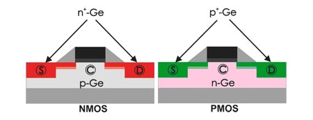 |
| The figure shows schematically the application of germanium in a CMOS (complementary metal oxide semiconductor) circuit. Note that germanium is only used in the regions of source (S), drain (D) and channel (C). Source and drain contain high concentration of foreign atoms (dopants) which provide the excess of free electrons (n+ regions) or holes (p+ regions). |
Abstract:
The use of germanium instead of silicon as basic material of transistors would enable faster chips containing smaller transistors.
A step towards germanium nanoelectronics
Dresden | Posted on February 17th, 2010However, a number of problems still have to be solved. Transistors are produced using foreign atoms that are implanted into the semiconductor material so that it becomes partly conducting. As this production step damages the material, it has to be repaired by subsequent annealing. So far it has not been possible to produce large-scale integrated transistors of a specific type (NMOS) using germanium. The reason: phosphorus atoms are strongly redistributed within the material during annealing. Two novel techniques, which were applied by scientists of the research center Forschungszentrum Dresden-Rossendorf (FZD) and international colleagues, overcome this dilemma. The results were published in Applied Physics Letters and Physical Review Letters.
Higher switching speeds than in silicon could be achieved using germanium and some other semiconductors. Germanium is particularly attractive since it could be easily integrated into existing technological processes. Germanium was the basic material of first-generation transistors before it was replaced by silicon at the end of the 1960s. This was due to the excellent electronic properties of the interface between the semiconductor silicon and its insulating and passivating oxide. However, this advantage cannot be utilized if transistor dimensions are further reduced since the oxide must then be replaced by so-called high-k dielectrics. This again stimulates science and industry to search for the most suitable basic material.
By inserting foreign atoms the conductivity of semiconductors can be varied in a purposeful way. One possibility is ion implantation (ions are charged atoms) with subsequent heat treatment, which is called annealing. Annealing of the germanium crystal is necessary as the material is heavily damaged during implantation, and leads to the requested electronic properties. While these methods allow for the manufacturing of p-channel transistors (PMOS) according to future technology needs (22 nanometer technology node), it was not possible to produce corresponding n-channel transistors (NMOS) using germanium. This is due to the strong spatial redistribution (diffusion) of the phosphorus atoms which have to be used in manufacturing the n+ regions.
Physicists from the FZD applied a special annealing method that enables repairing the germanium crystal and yields good electrical properties without the diffusion of phosphorus atoms. The germanium samples were heated by short light pulses of only a few milliseconds. This period is sufficient in order to restore the crystal quality and to achieve electrical activation of phosphorus, but it is too short for the spatial redistribution of the phosphorus atoms. The light pulses were generated by the flash lamp equipment which was developed at the research center FZD. Analysis of the electrical and structural properties of the thin phosphorus-doped layers in germanium was performed in close collaboration with colleagues from the Belgian microelectronics center IMEC in Leuven and from the Fraunhofer-Center for Nanoelectronic Technologies (CNT) in Dresden.
An alternative method to suppress phosphorus diffusion in germanium has been investigated by an international team consisting of researchers from Germany, Denmark and the USA, amongst them physicists from FZD. After ion implantation of phosphorus into germanium the sample was heated to a given temperature and then irradiated by protons. It could be demonstrated that this treatment leads to the reduction of phosphorus diffusion, too. The results of these experiments are explained by the influence of certain lattice defects (self-interstitials) that annihilate those lattice defects (vacancies) which are responsible for the mobility of the phosphorus atoms.
Thus, FZD physicists and their colleagues demonstrated that in principle it is possible to fabricate germanium-based n-channel transistors (NMOS) with dimensions corresponding to the most advanced technological requirements.
(Authors: Dr. Matthias Posselt / Dr. Christine Bohnet)
Publications:
C. W�ndisch, M. Posselt, B. Schmidt, V. Heera, T. Schumann, A. M�cklich, R. Gr�tzschel, W. Skorupa, T. Clarysse, E. Simoen, H. Hortenbach, "Millisecond flash lamp annealing of shallow implanted layers in Ge", in: Applied Physics Letters. 95 (2009), 252107. DOI: 10.1063/1.3276770.
H. Bracht, S. Schneider, J. N. Klug, C. Y. Liao, J. Lundsgaard Hansen, E. E. Haller, A. Nylandsted Larsen, D. Bougeard, M. Posselt, C. W�ndisch, "Interstitial-Mediated Diffusion in Germanium under Proton Irradiation", in: Physical Review Letters 103 (2009), 255501, DOI: 10.1103/PhysRevLett.103.255501.
####
About Forschungszentrum Dresden Rossendorf
The Forschungszentrum Dresden-Rossendorf, now a member of the Leibniz Association, will become new member of the Helmholtz Association as of January 2011. It is engaged in basic and application-oriented research.
For more information, please click here
Contacts:
Dr. Matthias Posselt / Clemens W�ndisch
Institute of Ion Beam Physics and Materials Research
Forschungszentrum Dresden-Rossendorf
Phone: ++49 351 260 - 3279 / - 3032
Contact to the media:
Dr. Christine Bohnet
Public relations
Bautzner Landstr. 400, 01328 Dresden
Phone: ++49 351 260 - 2450
++49 160 969 288 56
Fax: ++49 351 260 - 2700
Copyright © Forschungszentrum Dresden Rossendorf
If you have a comment, please Contact us.Issuers of news releases, not 7th Wave, Inc. or Nanotechnology Now, are solely responsible for the accuracy of the content.
Bookmark:


| Related News Press |
News and information
![]() Simulating magnetization in a Heisenberg quantum spin chain April 5th, 2024
Simulating magnetization in a Heisenberg quantum spin chain April 5th, 2024
![]() NRL charters Navy�s quantum inertial navigation path to reduce drift April 5th, 2024
NRL charters Navy�s quantum inertial navigation path to reduce drift April 5th, 2024
![]() Discovery points path to flash-like memory for storing qubits: Rice find could hasten development of nonvolatile quantum memory April 5th, 2024
Discovery points path to flash-like memory for storing qubits: Rice find could hasten development of nonvolatile quantum memory April 5th, 2024
Possible Futures
![]() Discovery points path to flash-like memory for storing qubits: Rice find could hasten development of nonvolatile quantum memory April 5th, 2024
Discovery points path to flash-like memory for storing qubits: Rice find could hasten development of nonvolatile quantum memory April 5th, 2024
![]() With VECSELs towards the quantum internet Fraunhofer: IAF achieves record output power with VECSEL for quantum frequency converters April 5th, 2024
With VECSELs towards the quantum internet Fraunhofer: IAF achieves record output power with VECSEL for quantum frequency converters April 5th, 2024
Chip Technology
![]() Discovery points path to flash-like memory for storing qubits: Rice find could hasten development of nonvolatile quantum memory April 5th, 2024
Discovery points path to flash-like memory for storing qubits: Rice find could hasten development of nonvolatile quantum memory April 5th, 2024
![]() Utilizing palladium for addressing contact issues of buried oxide thin film transistors April 5th, 2024
Utilizing palladium for addressing contact issues of buried oxide thin film transistors April 5th, 2024
![]() HKUST researchers develop new integration technique for efficient coupling of III-V and silicon February 16th, 2024
HKUST researchers develop new integration technique for efficient coupling of III-V and silicon February 16th, 2024
Nanoelectronics
![]() Interdisciplinary: Rice team tackles the future of semiconductors Multiferroics could be the key to ultralow-energy computing October 6th, 2023
Interdisciplinary: Rice team tackles the future of semiconductors Multiferroics could be the key to ultralow-energy computing October 6th, 2023
![]() Key element for a scalable quantum computer: Physicists from Forschungszentrum J�lich and RWTH Aachen University demonstrate electron transport on a quantum chip September 23rd, 2022
Key element for a scalable quantum computer: Physicists from Forschungszentrum J�lich and RWTH Aachen University demonstrate electron transport on a quantum chip September 23rd, 2022
![]() Reduced power consumption in semiconductor devices September 23rd, 2022
Reduced power consumption in semiconductor devices September 23rd, 2022
![]() Atomic level deposition to extend Moore�s law and beyond July 15th, 2022
Atomic level deposition to extend Moore�s law and beyond July 15th, 2022
Announcements
![]() NRL charters Navy�s quantum inertial navigation path to reduce drift April 5th, 2024
NRL charters Navy�s quantum inertial navigation path to reduce drift April 5th, 2024
![]() Discovery points path to flash-like memory for storing qubits: Rice find could hasten development of nonvolatile quantum memory April 5th, 2024
Discovery points path to flash-like memory for storing qubits: Rice find could hasten development of nonvolatile quantum memory April 5th, 2024
|
|
||
|
|
||
| The latest news from around the world, FREE | ||
|
|
||
|
|
||
| Premium Products | ||
|
|
||
|
Only the news you want to read!
Learn More |
||
|
|
||
|
Full-service, expert consulting
Learn More |
||
|
|
||