Home > Press > Research at UAlbany NanoCollege Contributes to Over 40 Technical Papers at Leading Global Lithography Forum
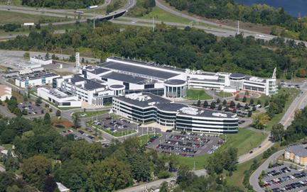 |
| CNSE's Albany NanoTech Complex |
Abstract:
Innovative work by researchers from CNSE and its global corporate partners at CNSE's Albany NanoTech Complex to be featured at SPIE Advanced Lithography Conference
Research at UAlbany NanoCollege Contributes to Over 40 Technical Papers at Leading Global Lithography Forum
Albany, NY | Posted on February 16th, 2010Innovative research conducted at the College of Nanoscale Science and Engineering's ("CNSE") Albany NanoTech ("ANT") Complex provides the basis for more than 40 scientific and technical papers to be presented next week at one of the world's leading conferences focused on advanced lithography.
The papers will be introduced at the SPIE Advanced Lithography conference, to be held February 21 through 25 in San Jose, CA. They cite leading-edge research performed by CNSE research teams; by global corporate partners' research teams resident at CNSE, including IBM, SEMATECH, GlobalFoundries, Tokyo Electron, Applied Materials, ASML, Vistec Lithography and the National Institute of Standards and Technology ("NIST"); and through collaborative programs involving the UAlbany NanoCollege and its corporate partners' research teams located at CNSE's ANT Complex.
Cutting-edge innovations designed to address a host of critical lithography challenges are outlined in a variety of technical areas, including advanced photoresist materials, mask blanks and process technologies for extreme ultraviolet ("EUV") lithography; double-patterning techniques for optical microlithography; lithographic techniques for self-assembly; and advances in electron-beam ("e-beam") lithography, nanometrology, and nanoimprint technologies, among others.
Dr. Timothy Groves, CNSE Empire Innovation Professor of Nanoscale Science and Director of CNSE's Center for Nanolithography Development, said, "The presentation of more than 40 scientific and technical papers at the SPIE Advanced Lithography conference based on research performed at CNSE's Albany NanoTech Complex further demonstrates the success of pioneering partnerships between academia and industry in driving cutting-edge research and development. These collaborations are clearly enabling critical innovations in nanoscale lithography that will serve to meet the needs of the global nanoelectronics industry."
Dr. John Hartley, CNSE Professor of Nanoengineering and Director of CNSE's Advanced Lithography Center, said, "The groundbreaking work being done at the UAlbany NanoCollege, from researchers both at CNSE and our world-class roster of global corporate partners, is playing an important role in accelerating the use of lithography technologies for the manufacturing of advanced nanoelectronics devices. We look forward to presenting the results of that leading-edge research and are confident it will enable critical lithography solutions for the benefit of our industrial partners and the industry as a whole."
The 35th annual SPIE conference - considered the nanoelectronics lithography industry's most important technical event - is expected to attract thousands of attendees.
####
About UAlbany NanoCollege
The UAlbany CNSE is the first college in the world dedicated to education, research, development, and deployment in the emerging disciplines of nanoscience, nanoengineering, nanobioscience, and nanoeconomics. CNSE's Albany NanoTech Complex is the most advanced research enterprise of its kind at any university in the world. With over $5.5 billion in high-tech investments, the 800,000-square-foot complex attracts corporate partners from around the world and offers students a one-of-a-kind academic experience. The UAlbany NanoCollege houses the only fully-integrated, 300mm wafer, computer chip pilot prototyping and demonstration line within 80,000 square feet of Class 1 capable cleanrooms. More than 2,500 scientists, researchers, engineers, students, and faculty work on site at CNSE's Albany NanoTech, from companies including IBM, AMD, GlobalFoundries, SEMATECH, Toshiba, Applied Materials, Tokyo Electron, ASML, Novellus Systems, Vistec Lithography and Atotech.
For more information, please click here
Contacts:
Steve Janack
CNSE Vice President for Marketing and Communications
(phone) 518-956-7322
(cell) 518-312-5009
Copyright © UAlbany NanoCollege
If you have a comment, please Contact us.Issuers of news releases, not 7th Wave, Inc. or Nanotechnology Now, are solely responsible for the accuracy of the content.
Bookmark:


| Related News Press |
News and information
![]() Simulating magnetization in a Heisenberg quantum spin chain April 5th, 2024
Simulating magnetization in a Heisenberg quantum spin chain April 5th, 2024
![]() NRL charters Navy�s quantum inertial navigation path to reduce drift April 5th, 2024
NRL charters Navy�s quantum inertial navigation path to reduce drift April 5th, 2024
![]() Discovery points path to flash-like memory for storing qubits: Rice find could hasten development of nonvolatile quantum memory April 5th, 2024
Discovery points path to flash-like memory for storing qubits: Rice find could hasten development of nonvolatile quantum memory April 5th, 2024
Chip Technology
![]() Discovery points path to flash-like memory for storing qubits: Rice find could hasten development of nonvolatile quantum memory April 5th, 2024
Discovery points path to flash-like memory for storing qubits: Rice find could hasten development of nonvolatile quantum memory April 5th, 2024
![]() Utilizing palladium for addressing contact issues of buried oxide thin film transistors April 5th, 2024
Utilizing palladium for addressing contact issues of buried oxide thin film transistors April 5th, 2024
![]() HKUST researchers develop new integration technique for efficient coupling of III-V and silicon February 16th, 2024
HKUST researchers develop new integration technique for efficient coupling of III-V and silicon February 16th, 2024
Nanoelectronics
![]() Interdisciplinary: Rice team tackles the future of semiconductors Multiferroics could be the key to ultralow-energy computing October 6th, 2023
Interdisciplinary: Rice team tackles the future of semiconductors Multiferroics could be the key to ultralow-energy computing October 6th, 2023
![]() Key element for a scalable quantum computer: Physicists from Forschungszentrum J�lich and RWTH Aachen University demonstrate electron transport on a quantum chip September 23rd, 2022
Key element for a scalable quantum computer: Physicists from Forschungszentrum J�lich and RWTH Aachen University demonstrate electron transport on a quantum chip September 23rd, 2022
![]() Reduced power consumption in semiconductor devices September 23rd, 2022
Reduced power consumption in semiconductor devices September 23rd, 2022
![]() Atomic level deposition to extend Moore�s law and beyond July 15th, 2022
Atomic level deposition to extend Moore�s law and beyond July 15th, 2022
Announcements
![]() NRL charters Navy�s quantum inertial navigation path to reduce drift April 5th, 2024
NRL charters Navy�s quantum inertial navigation path to reduce drift April 5th, 2024
![]() Discovery points path to flash-like memory for storing qubits: Rice find could hasten development of nonvolatile quantum memory April 5th, 2024
Discovery points path to flash-like memory for storing qubits: Rice find could hasten development of nonvolatile quantum memory April 5th, 2024
Interviews/Book Reviews/Essays/Reports/Podcasts/Journals/White papers/Posters
![]() Simulating magnetization in a Heisenberg quantum spin chain April 5th, 2024
Simulating magnetization in a Heisenberg quantum spin chain April 5th, 2024
![]() Discovery points path to flash-like memory for storing qubits: Rice find could hasten development of nonvolatile quantum memory April 5th, 2024
Discovery points path to flash-like memory for storing qubits: Rice find could hasten development of nonvolatile quantum memory April 5th, 2024
Events/Classes
![]() Researchers demonstrate co-propagation of quantum and classical signals: Study shows that quantum encryption can be implemented in existing fiber networks January 20th, 2023
Researchers demonstrate co-propagation of quantum and classical signals: Study shows that quantum encryption can be implemented in existing fiber networks January 20th, 2023
|
|
||
|
|
||
| The latest news from around the world, FREE | ||
|
|
||
|
|
||
| Premium Products | ||
|
|
||
|
Only the news you want to read!
Learn More |
||
|
|
||
|
Full-service, expert consulting
Learn More |
||
|
|
||