Home > Press > Made in IBM Labs: IBM Scientists Demonstrate World's Fastest Graphene Transistor
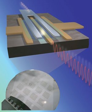 |
| IBM Graphene RF Transistor |
Abstract:
Holds Promise for Improving Performance of Transistors
Made in IBM Labs: IBM Scientists Demonstrate World's Fastest Graphene Transistor
Yorktown Heights, NY | Posted on February 5th, 2010In a just-published paper in the magazine Science, IBM (NYSE: IBM) researchers demonstrated a radio-frequency graphene transistor with the highest cut-off frequency achieved so far for any graphene device - 100 billion cycles/second (100 GigaHertz).
This accomplishment is a key milestone for the Carbon Electronics for RF Applications (CERA) program funded by DARPA, in an effort to develop next-generation communication devices.
The high frequency record was achieved using wafer-scale, epitaxially grown graphene using processing technology compatible to that used in advanced silicon device fabrication.
"A key advantage of graphene lies in the very high speeds in which electrons propagate, which is essential for achieving high-speed, high-performance next generation transistors," said Dr. T.C. Chen, vice president, Science and Technology, IBM Research. "The breakthrough we are announcing demonstrates clearly that graphene can be utilized to produce high performance devices and integrated circuits."
Graphene is a single atom-thick layer of carbon atoms bonded in a hexagonal honeycomb-like arrangement. This two-dimensional form of carbon has unique electrical, optical, mechanical and thermal properties and its technological applications are being explored intensely.
Uniform and high-quality graphene wafers were synthesized by thermal decomposition of a silicon carbide (SiC) substrate. The graphene transistor itself utilized a metal top-gate architecture and a novel gate insulator stack involving a polymer and a high dielectric constant oxide. The gate length was modest, 240 nanometers, leaving plenty of space for further optimization of its performance by scaling down the gate length.
It is noteworthy that the frequency performance of the graphene device already exceeds the cut-off frequency of state-of-the-art silicon transistors of the same gate length (~ 40 GigaHertz). Similar performance was obtained from devices based on graphene obtained from natural graphite, proving that high performance can be obtained from graphene of different origins. Previously, the team had demonstrated graphene transistors with a cut-off frequency of 26 GigaHertz using graphene flakes extracted from natural graphite.
####
For more information, please click here
Contacts:
Michael Loughran
IBM Media Relations
914-945-1613
Copyright © IBM
If you have a comment, please Contact us.Issuers of news releases, not 7th Wave, Inc. or Nanotechnology Now, are solely responsible for the accuracy of the content.
Bookmark:


| Related News Press |
News and information
![]() Simulating magnetization in a Heisenberg quantum spin chain April 5th, 2024
Simulating magnetization in a Heisenberg quantum spin chain April 5th, 2024
![]() NRL charters Navy�s quantum inertial navigation path to reduce drift April 5th, 2024
NRL charters Navy�s quantum inertial navigation path to reduce drift April 5th, 2024
![]() Discovery points path to flash-like memory for storing qubits: Rice find could hasten development of nonvolatile quantum memory April 5th, 2024
Discovery points path to flash-like memory for storing qubits: Rice find could hasten development of nonvolatile quantum memory April 5th, 2024
Possible Futures
![]() Discovery points path to flash-like memory for storing qubits: Rice find could hasten development of nonvolatile quantum memory April 5th, 2024
Discovery points path to flash-like memory for storing qubits: Rice find could hasten development of nonvolatile quantum memory April 5th, 2024
![]() With VECSELs towards the quantum internet Fraunhofer: IAF achieves record output power with VECSEL for quantum frequency converters April 5th, 2024
With VECSELs towards the quantum internet Fraunhofer: IAF achieves record output power with VECSEL for quantum frequency converters April 5th, 2024
Chip Technology
![]() Discovery points path to flash-like memory for storing qubits: Rice find could hasten development of nonvolatile quantum memory April 5th, 2024
Discovery points path to flash-like memory for storing qubits: Rice find could hasten development of nonvolatile quantum memory April 5th, 2024
![]() Utilizing palladium for addressing contact issues of buried oxide thin film transistors April 5th, 2024
Utilizing palladium for addressing contact issues of buried oxide thin film transistors April 5th, 2024
![]() HKUST researchers develop new integration technique for efficient coupling of III-V and silicon February 16th, 2024
HKUST researchers develop new integration technique for efficient coupling of III-V and silicon February 16th, 2024
Nanoelectronics
![]() Interdisciplinary: Rice team tackles the future of semiconductors Multiferroics could be the key to ultralow-energy computing October 6th, 2023
Interdisciplinary: Rice team tackles the future of semiconductors Multiferroics could be the key to ultralow-energy computing October 6th, 2023
![]() Key element for a scalable quantum computer: Physicists from Forschungszentrum J�lich and RWTH Aachen University demonstrate electron transport on a quantum chip September 23rd, 2022
Key element for a scalable quantum computer: Physicists from Forschungszentrum J�lich and RWTH Aachen University demonstrate electron transport on a quantum chip September 23rd, 2022
![]() Reduced power consumption in semiconductor devices September 23rd, 2022
Reduced power consumption in semiconductor devices September 23rd, 2022
![]() Atomic level deposition to extend Moore�s law and beyond July 15th, 2022
Atomic level deposition to extend Moore�s law and beyond July 15th, 2022
Announcements
![]() NRL charters Navy�s quantum inertial navigation path to reduce drift April 5th, 2024
NRL charters Navy�s quantum inertial navigation path to reduce drift April 5th, 2024
![]() Discovery points path to flash-like memory for storing qubits: Rice find could hasten development of nonvolatile quantum memory April 5th, 2024
Discovery points path to flash-like memory for storing qubits: Rice find could hasten development of nonvolatile quantum memory April 5th, 2024
|
|
||
|
|
||
| The latest news from around the world, FREE | ||
|
|
||
|
|
||
| Premium Products | ||
|
|
||
|
Only the news you want to read!
Learn More |
||
|
|
||
|
Full-service, expert consulting
Learn More |
||
|
|
||