Home > Press > New Singapore-French nanotech lab opens at NTU
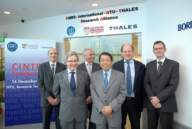 |
| Strengthening the collaborative R&D relationship between Singapore and France. Front row, from left: His Excellency Mr Olivier Caron, Ambassador of France to Singapore; and Dr Su Guaning, President NTU. Back row, from left: Mr Pierre Guillon, Director, Institute for Engineering and Systems Science, CNRS; Mr Patrick Plante, Chief Executive Officer, Thales Technology Centre Singapore; Professor Bertil Andersson, Provost NTU; and Professor Dominique Baillargeat, Director CINTRA. |
Abstract:
Unique joint set-up by a research centre, a university and a private organisation
New Singapore-French nanotech lab opens at NTU
Singapore & France | Posted on December 16th, 2009Just two months after the Nanyang Technological University (NTU) signed the Memorandum of Understanding in Paris with the National Center for Scientific Research (CNRS) and the Thales Group of Companies to set up a joint research laboratory, the three parties are meeting again in Singapore to inaugurate the CNRS-International-NTU-Thales Research Alliance (CINTRA) Laboratory at NTU.
Located at the Research Techno Plaza, the CINTRA Laboratory aims to harness the latest in science and technology to develop innovations in nanotechnologies for computing, sensing and communications applications.
Over the next two years, about 50 Singapore and French researchers will work on critical issues and challenges faced by existing technologies in the microelectronic and photonic industries, promising innovations to meet future commercial as well as defence and security needs.
Examples of such application-driven challenges include the development of enabling technologies such as an imaging chip to process and display real-time multi-dimensional information, and a low-power signal processing chip capable of super high-speed performance of a trillion bits (terabit) per second or more.
His Excellency Mr Olivier Caron, the Ambassador of France to Singapore, who was the guest-of-honour at the inauguration ceremony, said: "The R&D and innovation landscapes have changed, and are no longer confined to simple projects that can be defined, funded and conducted within single companies, universities or research institutions. It is no longer possible to progress in a major field of scientific research without the cooperation and strong commitment of different actors coming from different regions of the world."
"France and Singapore have long ago started this process of collaborative work and mutual aid, launching different research projects and tightening the R&D relationships between both countries," said Mr Caron. "This current alliance is unlike most of the others - it brings together a research centre, a university and a private company in the same location. Academia, fundamental research, applied research, and technology transfer are considered in this union. This model should not only drive breakthroughs in innovation but should also result in bringing these innovations to the market."
NTU President Dr Su Guaning said: "NTU is acknowledged as a University that seeks to be relevant to the needs of industry, innovating and pioneering new application areas while building on our staff's core competencies. We seek to be nimble, listening closely to the research trends while responding to the needs of the industry."
"We are indeed grateful to CNRS and Thales for the confidence that they have shown in NTU. Together with CNRS' strength in research and Thales' experience in the global market, we shall make the CINTRA Laboratory an example of how upstream research can turn into successful commercial products and applications in a most unexpected way," said Dr Su.
Mr Jean-Jacques Gagnepain, Adviser to the CNRS President on International Affairs, said: "CNRS salutes the impressive commitment that NTU has granted to our joint laboratory, the Unit� Mixte Internationale CINTRA."
"Within these superb, well-designed and ergonomic premises that we visited today, we feel all the more certain that the joint efforts of our scientists will allow NTU, Thales and CNRS to produce far-reaching research results, concepts and inventions. It is our joint ambition to lift the bottlenecks that currently block existing microelectronic and photonic research," said Mr Gagnepain.
Mr Patrick Plante, Chief Executive Officer of Thales Technology Centre Singapore, said: "Thales reaffirms its strong commitment to the Unit� Mixte Internationale CINTRA and is proud to be one of the three pillars of this unique joint collaboration between academic, research and industry partners outside of France."
"Our long-standing relationship with the prestigious NTU of Singapore established since the creation of our joint research lab as well as our long-valued partnership with the largest fundamental research organisation in Europe, CNRS, will be significantly reinforced, and we trust that our complementarities will lead CINTRA to excellence in developing cutting-edge technologies. In this research-friendly environment at NTU, CINTRA will fly the flag for French-Singapore advanced research on nanotechnologies and nanophotonics," said Mr Plante.
####
About Nanyang Technological University
Nanyang Technological University (NTU) is a research-intensive university with globally acknowledged strengths in science and engineering. The university has roots that go back to 1955 when Nanyang University was set up. Today, NTU has four colleges with 12 schools, and three autonomous entities, the National Institute of Education, the S Rajaratnam School of International Studies, and the Earth Observatory of Singapore.
For more information, please click here
Contacts:
Media Contact:
Edgar Lee
Senior Assistant Director
Corporate Communications Office
Nanyang Technological University
Tel: (+65) 6790 6052
Mobile: (+65) 8322 3973
Copyright © Nanyang Technological University
If you have a comment, please Contact us.Issuers of news releases, not 7th Wave, Inc. or Nanotechnology Now, are solely responsible for the accuracy of the content.
Bookmark:


| Related News Press |
News and information
![]() Quantum computer improves AI predictions April 17th, 2026
Quantum computer improves AI predictions April 17th, 2026
![]() Flexible sensor gains sensitivity under pressure April 17th, 2026
Flexible sensor gains sensitivity under pressure April 17th, 2026
![]() A reusable chip for particulate matter sensing April 17th, 2026
A reusable chip for particulate matter sensing April 17th, 2026
![]() Detecting vibrational quantum beating in the predissociation dynamics of SF6 using time-resolved photoelectron spectroscopy April 17th, 2026
Detecting vibrational quantum beating in the predissociation dynamics of SF6 using time-resolved photoelectron spectroscopy April 17th, 2026
Academic/Education
![]() Rice University launches Rice Synthetic Biology Institute to improve lives January 12th, 2024
Rice University launches Rice Synthetic Biology Institute to improve lives January 12th, 2024
![]() Multi-institution, $4.6 million NSF grant to fund nanotechnology training September 9th, 2022
Multi-institution, $4.6 million NSF grant to fund nanotechnology training September 9th, 2022
Announcements
![]() A fundamentally new therapeutic approach to cystic fibrosis: Nanobody repairs cellular defect April 17th, 2026
A fundamentally new therapeutic approach to cystic fibrosis: Nanobody repairs cellular defect April 17th, 2026
![]() UC Irvine physicists discover method to reverse �quantum scrambling� : The work addresses the problem of information loss in quantum computing system April 17th, 2026
UC Irvine physicists discover method to reverse �quantum scrambling� : The work addresses the problem of information loss in quantum computing system April 17th, 2026
Homeland Security
![]() The picture of health: Virginia Tech researchers enhance bioimaging and sensing with quantum photonics June 30th, 2023
The picture of health: Virginia Tech researchers enhance bioimaging and sensing with quantum photonics June 30th, 2023
![]() Sensors developed at URI can identify threats at the molecular level: More sensitive than a dog's nose and the sensors don't get tired May 21st, 2021
Sensors developed at URI can identify threats at the molecular level: More sensitive than a dog's nose and the sensors don't get tired May 21st, 2021
![]() Highly sensitive dopamine detector uses 2D materials August 7th, 2020
Highly sensitive dopamine detector uses 2D materials August 7th, 2020
Military
![]() Quantum engineers �squeeze� laser frequency combs to make more sensitive gas sensors January 17th, 2025
Quantum engineers �squeeze� laser frequency combs to make more sensitive gas sensors January 17th, 2025
![]() Chainmail-like material could be the future of armor: First 2D mechanically interlocked polymer exhibits exceptional flexibility and strength January 17th, 2025
Chainmail-like material could be the future of armor: First 2D mechanically interlocked polymer exhibits exceptional flexibility and strength January 17th, 2025
![]() Single atoms show their true color July 5th, 2024
Single atoms show their true color July 5th, 2024
![]() NRL charters Navy�s quantum inertial navigation path to reduce drift April 5th, 2024
NRL charters Navy�s quantum inertial navigation path to reduce drift April 5th, 2024
Photonics/Optics/Lasers
![]() Metasurfaces smooth light to boost magnetic sensing precision January 30th, 2026
Metasurfaces smooth light to boost magnetic sensing precision January 30th, 2026
![]() From sensors to smart systems: the rise of AI-driven photonic noses January 30th, 2026
From sensors to smart systems: the rise of AI-driven photonic noses January 30th, 2026
Alliances/Trade associations/Partnerships/Distributorships
![]() Chicago Quantum Exchange welcomes six new partners highlighting quantum technology solutions, from Chicago and beyond September 23rd, 2022
Chicago Quantum Exchange welcomes six new partners highlighting quantum technology solutions, from Chicago and beyond September 23rd, 2022
![]() University of Illinois Chicago joins Brookhaven Lab's Quantum Center June 10th, 2022
University of Illinois Chicago joins Brookhaven Lab's Quantum Center June 10th, 2022
|
|
||
|
|
||
| The latest news from around the world, FREE | ||
|
|
||
|
|
||
| Premium Products | ||
|
|
||
|
Only the news you want to read!
Learn More |
||
|
|
||
|
Full-service, expert consulting
Learn More |
||
|
|
||