Home > Press > New semiconductor laser structure could produce more efficient, powerful and portable sources emitting in the mid-infrared
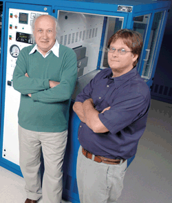 |
| Professors Dan Botez and Luke Mawst |
Abstract:
University of Wisconsin-Madison researchers have achieved a nanoscale laser structure they anticipate will produce semiconductor lasers in the next two years that are more than twice as efficient as current continuous-wave lasers emitting in the mid-infrared.
New semiconductor laser structure could produce more efficient, powerful and portable sources emitting in the mid-infrared
Madison, WI | Posted on December 8th, 2009"The novel structure will produce lasers with more power and that are more efficient, reliable and stable," says Philip Dunham Reed Professor of Electrical and Computer Engineering Dan Botez, who created the new structure with Electrical and Computer Engineering Professor Luke Mawst.
These next-generation lasers could benefit a wide range of industries, as they could be used in biomedical devices, environmental monitoring devices, missile avoidance systems and even food packaging processes. This wide range of applications is possible because the researchers have all but eliminated the temperature sensitivity for lasers operating in continuous-wave mode, meaning the laser emits uninterrupted, coherent light.
"For example, with current mid-infrared technologies for detecting explosives, lasers can detect from only approximately 30 feet away," Botez says. "With these lasers, devices could detect explosives at more like 300 feet away."
Also important is that the researchers created the new laser structure via a scalable industrial process.
How is a regular semiconductor laser built?
Researchers can harness electron movement to produce a laser. In a free-floating atom, electrons orbit in rings closer to or farther from the nucleus, depending on how much energy the electron is carrying. In a solid, atoms are fixed in a lattice (like a complex chain or pattern), and electrons move in and jump between energy bands instead of between the fixed energy levels corresponding to the various orbits in free atoms. In semiconducting materials, electrons can move into an energy band, called a conduction band, which produces a current. They can also move inside a band called a valence band that is so jam-packed with electrons that no net current flow happens. Electrons can easily be stimulated to move to the conduction band�but to maintain equilibrium, they eventually have to return to the valence band to fill in the "holes". they left behind. The electron returns to the valence band via a port or "well" in the conduction band, which dips closer to the valence band in a region called the "active region". As that occurs, the electron gives off its excess energy, sometimes in the form of a photon, which is a quantum of light. (A quantum of something is the smallest discrete quantity possible.)
Electrons that spontaneously move between bands and produce light can be used for devices like LEDs. However, to produce a laser beam, researchers place the lattice of atoms in a cavity with mirrors, and the generated photons stimulate the electrons to return to the valence band, thus releasing a photon with the same energy as the stimulating one. The original photon and the new photon are in phase with each other and will further stimulate the release of other photons, thus continuously amplifying the number of photons and bouncing off the cavity mirrors. The process repeats until the cavity reaches a threshold for oscillation and light is directed out of the cavity in a coherent laser beam.
This is how a standard semiconductor laser works, but the problem is that band-to-band transitions are limited to wavelengths below approximately three microns, which correspond to transition energies of about .4 electron volts. If the transition energies are smaller, which would correspond to longer wavelengths, the energy is released as heat, rather than light�meaning traditional semiconductor lasers have limited emitted-light wavelength potential.
A move forward: quantum cascade lasers
To overcome wavelength limitations, scientists from Bell Laboratories developed a laser by quantizing the energy bands, meaning they broke the energy bands into sub-bands. As the lattice structure vibrates, it causes the electrons to move rapidly between sub-bands, and the transitions between sub-bands cause the electrons to emit energy. However, the process is extremely inefficient since electrons transitioning between two sub-bands emit 1,000 phonons (quantized lattice vibrations) for every one photon. Bell Labs scientists reduced this inefficiency by creating a "cascade" structure by .stacking. 40 sub-band photon-emitting stages. These stages allow one electron to be used to emit a photon 40 times as it sequentially moves and transitions along the cascade structure. The result is only 25 phonons are emitted for every one emitted photon and then lasing action can be achieved.
The problem with this type of laser is that fixed compositions of the layers for a particular stage, which repeats along the cascade structure, result in electrons escaping from the structure. Imagine dropping a ball down a ladder; the ball may hit the first couple of steps, or sub-bands, but as it progresses along the ladder, it can veer off course and drop off the ladder entirely. A continuous-wave laser system, which operates continuously, heats up internally as electrons escape from the structure, which in turn limits the emitted power and the overall device efficiency.
This loss of electrons, or carrier leakage, has been a major barrier to increasing laser efficiency for practical applications.
A solution: Deep-well quantum cascade lasers
About five years ago, a process for growing multi-layer semiconductor structures became available for fabricating quantum-cascade lasers. Called metalorganic chemical vapor deposition (MOCVD), the process is scalable, unlike previous crystal growth techniques suited for laboratories but not manufacturers. MOCVD involves exposing a substrate to high heat and chemicals, causing layers to form on the substrate in an atomic-lattice configuration. Unlike previous crystal-growth techniques, MOCVD allows researchers to fabricate cascade-laser structures with stages composed of layers of varying composition.
Botez and Mawst are using the MOCVD process to grow varying-composition structures that prevent carrier leakage. To compensate for the added strain caused in the structure by creating deeper (quantum) wells, they also create taller barriers. Now, rather than electrons escaping from the system like balls falling off a ladder, the system works like a set of tiered boxes, with a ball getting caught at each stage. This ensures that electrons will efficiently produce photons in every stage of the cascade structure. The new structure is called a deep-well quantum cascade laser.
"By suppressing carrier leakage, there is about 2.5 times less heating in the device while the laser is in continuous-wave operation," says Botez. "This is a dramatic improvement that means the device will be almost temperature insensitive".
The result will be continuous-wave lasers that Botez anticipates will achieve at least 20 percent wall-plug efficiency, which is the electrical-to-optical power efficiency of a laser system. Twenty percent efficiency would be roughly double the current world record for practical continuous-wave quantum cascade lasers.
This new structure, coupled with the fact that MOCVD is a process suitable for mass production, means that optimized mid-infrared lasers can become much more widespread in medicine, the military and a wide variety of industries.
"The effect will be that as you get more continuous wave power you should also get better long-term reliability and stability, because these lasers will be much less sensitive to temperature variations than conventional quantum cascade lasers," Botez says.
Botez and Mawst are actively interested in commercializing the technology, which is covered by two issued and one pending U.S. patents through the Wisconsin Alumni Research Foundation.
####
For more information, please click here
Copyright © University of Wisconsin-Madison College of Engineering
If you have a comment, please Contact us.Issuers of news releases, not 7th Wave, Inc. or Nanotechnology Now, are solely responsible for the accuracy of the content.
Bookmark:


| Related News Press |
News and information
![]() Quantum computer improves AI predictions April 17th, 2026
Quantum computer improves AI predictions April 17th, 2026
![]() Flexible sensor gains sensitivity under pressure April 17th, 2026
Flexible sensor gains sensitivity under pressure April 17th, 2026
![]() A reusable chip for particulate matter sensing April 17th, 2026
A reusable chip for particulate matter sensing April 17th, 2026
![]() Detecting vibrational quantum beating in the predissociation dynamics of SF6 using time-resolved photoelectron spectroscopy April 17th, 2026
Detecting vibrational quantum beating in the predissociation dynamics of SF6 using time-resolved photoelectron spectroscopy April 17th, 2026
Possible Futures
![]() A fundamentally new therapeutic approach to cystic fibrosis: Nanobody repairs cellular defect April 17th, 2026
A fundamentally new therapeutic approach to cystic fibrosis: Nanobody repairs cellular defect April 17th, 2026
![]() UC Irvine physicists discover method to reverse �quantum scrambling� : The work addresses the problem of information loss in quantum computing system April 17th, 2026
UC Irvine physicists discover method to reverse �quantum scrambling� : The work addresses the problem of information loss in quantum computing system April 17th, 2026
Announcements
![]() A fundamentally new therapeutic approach to cystic fibrosis: Nanobody repairs cellular defect April 17th, 2026
A fundamentally new therapeutic approach to cystic fibrosis: Nanobody repairs cellular defect April 17th, 2026
![]() UC Irvine physicists discover method to reverse �quantum scrambling� : The work addresses the problem of information loss in quantum computing system April 17th, 2026
UC Irvine physicists discover method to reverse �quantum scrambling� : The work addresses the problem of information loss in quantum computing system April 17th, 2026
Homeland Security
![]() The picture of health: Virginia Tech researchers enhance bioimaging and sensing with quantum photonics June 30th, 2023
The picture of health: Virginia Tech researchers enhance bioimaging and sensing with quantum photonics June 30th, 2023
![]() Sensors developed at URI can identify threats at the molecular level: More sensitive than a dog's nose and the sensors don't get tired May 21st, 2021
Sensors developed at URI can identify threats at the molecular level: More sensitive than a dog's nose and the sensors don't get tired May 21st, 2021
![]() Highly sensitive dopamine detector uses 2D materials August 7th, 2020
Highly sensitive dopamine detector uses 2D materials August 7th, 2020
Military
![]() Quantum engineers �squeeze� laser frequency combs to make more sensitive gas sensors January 17th, 2025
Quantum engineers �squeeze� laser frequency combs to make more sensitive gas sensors January 17th, 2025
![]() Chainmail-like material could be the future of armor: First 2D mechanically interlocked polymer exhibits exceptional flexibility and strength January 17th, 2025
Chainmail-like material could be the future of armor: First 2D mechanically interlocked polymer exhibits exceptional flexibility and strength January 17th, 2025
![]() Single atoms show their true color July 5th, 2024
Single atoms show their true color July 5th, 2024
![]() NRL charters Navy�s quantum inertial navigation path to reduce drift April 5th, 2024
NRL charters Navy�s quantum inertial navigation path to reduce drift April 5th, 2024
Food/Agriculture/Supplements
![]() New imaging approach transforms study of bacterial biofilms August 8th, 2025
New imaging approach transforms study of bacterial biofilms August 8th, 2025
![]() SMART researchers pioneer first-of-its-kind nanosensor for real-time iron detection in plants February 28th, 2025
SMART researchers pioneer first-of-its-kind nanosensor for real-time iron detection in plants February 28th, 2025
Environment
![]() A reusable chip for particulate matter sensing April 17th, 2026
A reusable chip for particulate matter sensing April 17th, 2026
![]() Researchers unveil a groundbreaking clay-based solution to capture carbon dioxide and combat climate change June 6th, 2025
Researchers unveil a groundbreaking clay-based solution to capture carbon dioxide and combat climate change June 6th, 2025
Nanobiotechnology
![]() A fundamentally new therapeutic approach to cystic fibrosis: Nanobody repairs cellular defect April 17th, 2026
A fundamentally new therapeutic approach to cystic fibrosis: Nanobody repairs cellular defect April 17th, 2026
![]() New molecular technology targets tumors and simultaneously silences two �undruggable� cancer genes August 8th, 2025
New molecular technology targets tumors and simultaneously silences two �undruggable� cancer genes August 8th, 2025
![]() New imaging approach transforms study of bacterial biofilms August 8th, 2025
New imaging approach transforms study of bacterial biofilms August 8th, 2025
![]() Electrifying results shed light on graphene foam as a potential material for lab grown cartilage June 6th, 2025
Electrifying results shed light on graphene foam as a potential material for lab grown cartilage June 6th, 2025
Photonics/Optics/Lasers
![]() Metasurfaces smooth light to boost magnetic sensing precision January 30th, 2026
Metasurfaces smooth light to boost magnetic sensing precision January 30th, 2026
![]() From sensors to smart systems: the rise of AI-driven photonic noses January 30th, 2026
From sensors to smart systems: the rise of AI-driven photonic noses January 30th, 2026
Quantum nanoscience
![]() Beyond silicon: Electronics at the scale of a single molecule January 30th, 2026
Beyond silicon: Electronics at the scale of a single molecule January 30th, 2026
![]() MXene nanomaterials enter a new dimension Multilayer nanomaterial: MXene flakes created at Drexel University show new promise as 1D scrolls January 30th, 2026
MXene nanomaterials enter a new dimension Multilayer nanomaterial: MXene flakes created at Drexel University show new promise as 1D scrolls January 30th, 2026
![]() ICFO researchers overcome long-standing bottleneck in single photon detection with twisted 2D materials August 8th, 2025
ICFO researchers overcome long-standing bottleneck in single photon detection with twisted 2D materials August 8th, 2025
|
|
||
|
|
||
| The latest news from around the world, FREE | ||
|
|
||
|
|
||
| Premium Products | ||
|
|
||
|
Only the news you want to read!
Learn More |
||
|
|
||
|
Full-service, expert consulting
Learn More |
||
|
|
||