Home > Press > KLA-Tencor Launches 8900 Inspection System: Flexible defect inspection system for CMOS image sensor applications
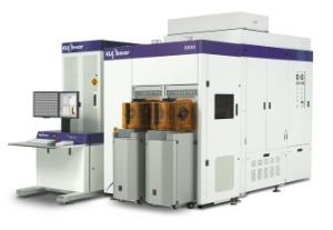 |
| KLA-Tencor's new 8900 high speed patterned-wafer defect inspection system represents a single-tool solution for image-sensor color filter and microlens development and production applications. (Photo: Business Wire) |
Abstract:
* The 8900 defect inspection system expands KLA-Tencor's product portfolio in CMOS image sensor process control
* The 8900 represents a single, flexible solution to address the wide range of defect challenges that arise during the manufacturing of an image sensor's color filter array
KLA-Tencor Launches 8900 Inspection System: Flexible defect inspection system for CMOS image sensor applications
Milpitas, CA | Posted on October 12th, 2009Today KLA-Tencor Corporation (NASDAQ:KLAC), the world's leading supplier of process control and yield management solutions for the semiconductor and related industries, extended its product offerings in the CMOS image sensor (CIS) market by announcing the 8900 defect inspection system. KLA-Tencor's new 8900 offers selectable illumination wavelengths, color-matched to CIS pixels; simultaneous brightfield and darkfield optical channels to enable capture of a wide variety of defect types; and adjustable sensitivity and throughput settings for cost-effective defect management from initial product development through volume production of color filter arrays (CFA).
Image sensors are devices that convert light into electrical signal, for use primarily in cameras. A color filter allows each pixel of the sensor to respond to a specific color�typically red, green or blue (RGB). The CFA is constructed in single-color, patterned layers, with one filter on top of each sensor pixel. Each pixel is capped with a micro-lens. As yield-limiting defects can occur at any step in the assembly process, the 8900's ability to inspect any of the filter or micro-lens layers can help reduce materials waste and cycle time.
An 8900 defect inspection system was recently installed at the first 300mm advanced CFA fab of Toppan Printing Company, Ltd., an industry leader in color filters. "State-of-the-art defect control is important to our ability to provide advanced color filters reliably," said Keiichi Hara, Chief Manager, On-chip Color Filter Department, Kumamoto Plant of Toppan Electronics Products Co., Ltd. "The 8900 has improved our defect control capability and changed our strategy. Because the 8900 is sensitive to a wide range of defect types and has high throughput, it is performing all the defect inspections in the CFA process. This previously required multiple inspection tools. The 8900 can also automate the defect monitoring tasks that used to require manual inspection, making our cycle times shorter and more predictable."
"Image sensor fabs have been using a combination of defect inspection systems, including manual inspection, to cover CFA process development, line monitoring, and incoming and outgoing quality control," remarked Oreste Donzella, Vice President and General Manager of the SWIFT division at KLA-Tencor. "This strategy can lead to errors and inefficiencies. For example, manual inspection results have high variability. Even with automated systems, critical defect excursions can be missed because the results are difficult to compare among different systems. In developing the 8900, we leveraged KLA-Tencor's extensive experience in brightfield and darkfield micro and macro inspection to provide image sensor fabs with a single, flexible system to address the breadth of their CFA inspection requirements. We believe that the 8900 will allow fabs to improve resource allocation, increase the yield of their current products and accelerate delivery of their latest image sensors."
Key features of the 8900 defect inspection system include:
* Simultaneous brightfield and darkfield optical paths to capture a wide range of defect types in a single pass, such as micro-lens deformation; resist and fall-on defects; color contamination; large stains and striations;
* Selectable LED inspection and review illumination spectrum matched to CIS filter colors;
* Sensitivity consistent with requirements of advanced CIS roadmaps;
* Throughput above 110 wafers per hour at production sensitivity, for 300mm semiconductor wafers;
* Automated binning of defects by type;
* Automated sensor pass/fail dispositioning; and
* Automated color review for defect verification.
For more technical details about the 8900, please visit the product webpage: www.kla-tencor.com/patterned-wafer/8900.html.
####
About KLA-Tencor Corporation
KLA-Tencor Corporation (NASDAQ:KLAC), a leading provider of process control and yield management solutions, partners with customers around the world to develop state-of-the-art inspection and metrology technologies. These technologies serve the semiconductor, data storage, compound semiconductor, photovoltaic, and other related nanoelectronics industries. With a portfolio of industry-standard products and a team of world-class engineers and scientists, the company has created superior solutions for its customers for over 30 years. Headquartered in Milpitas, California, KLA-Tencor has dedicated customer operations and service centers around the world.
Forward Looking Statements:
Statements in this press release other than historical facts, such as statements regarding the 8900�s expected performance (including its defect capture and the benefits that may be realized by our customers through the use of the 8900), are forward-looking statements, and are subject to the Safe Harbor provisions created by the Private Securities Litigation Reform Act of 1995. These forward-looking statements are based on current information and expectations, and involve a number of risks and uncertainties. Actual results may differ materially from those projected in such statements due to various factors, including delays in the adoption of new technologies (whether due to cost or performance issues or otherwise) or unanticipated technological challenges or limitations that affect the implementation or use of our products.
For more information, please click here
Contacts:
KLA-Tencor Corporation
Investor Relations:
Ed Lockwood
408-875-9529
Sr. Director, Investor Relations
Media Relations:
Meggan Powers
408-875-8733
Sr. Director, Corporate Communications
Copyright © Business Wire 2009
If you have a comment, please Contact us.Issuers of news releases, not 7th Wave, Inc. or Nanotechnology Now, are solely responsible for the accuracy of the content.
Bookmark:


| Related News Press |
News and information
![]() Quantum computer improves AI predictions April 17th, 2026
Quantum computer improves AI predictions April 17th, 2026
![]() Flexible sensor gains sensitivity under pressure April 17th, 2026
Flexible sensor gains sensitivity under pressure April 17th, 2026
![]() A reusable chip for particulate matter sensing April 17th, 2026
A reusable chip for particulate matter sensing April 17th, 2026
![]() Detecting vibrational quantum beating in the predissociation dynamics of SF6 using time-resolved photoelectron spectroscopy April 17th, 2026
Detecting vibrational quantum beating in the predissociation dynamics of SF6 using time-resolved photoelectron spectroscopy April 17th, 2026
Imaging
![]() Simple algorithm paired with standard imaging tool could predict failure in lithium metal batteries August 8th, 2025
Simple algorithm paired with standard imaging tool could predict failure in lithium metal batteries August 8th, 2025
Sensors
![]() Flexible sensor gains sensitivity under pressure April 17th, 2026
Flexible sensor gains sensitivity under pressure April 17th, 2026
![]() Tiny nanosheets, big leap: A new sensor detects ethanol at ultra-low levels January 30th, 2026
Tiny nanosheets, big leap: A new sensor detects ethanol at ultra-low levels January 30th, 2026
![]() From sensors to smart systems: the rise of AI-driven photonic noses January 30th, 2026
From sensors to smart systems: the rise of AI-driven photonic noses January 30th, 2026
![]() Sensors innovations for smart lithium-based batteries: advancements, opportunities, and potential challenges August 8th, 2025
Sensors innovations for smart lithium-based batteries: advancements, opportunities, and potential challenges August 8th, 2025
Announcements
![]() A fundamentally new therapeutic approach to cystic fibrosis: Nanobody repairs cellular defect April 17th, 2026
A fundamentally new therapeutic approach to cystic fibrosis: Nanobody repairs cellular defect April 17th, 2026
![]() UC Irvine physicists discover method to reverse �quantum scrambling� : The work addresses the problem of information loss in quantum computing system April 17th, 2026
UC Irvine physicists discover method to reverse �quantum scrambling� : The work addresses the problem of information loss in quantum computing system April 17th, 2026
Tools
![]() Metasurfaces smooth light to boost magnetic sensing precision January 30th, 2026
Metasurfaces smooth light to boost magnetic sensing precision January 30th, 2026
![]() From sensors to smart systems: the rise of AI-driven photonic noses January 30th, 2026
From sensors to smart systems: the rise of AI-driven photonic noses January 30th, 2026
![]() Japan launches fully domestically produced quantum computer: Expo visitors to experience quantum computing firsthand August 8th, 2025
Japan launches fully domestically produced quantum computer: Expo visitors to experience quantum computing firsthand August 8th, 2025
|
|
||
|
|
||
| The latest news from around the world, FREE | ||
|
|
||
|
|
||
| Premium Products | ||
|
|
||
|
Only the news you want to read!
Learn More |
||
|
|
||
|
Full-service, expert consulting
Learn More |
||
|
|
||