Home > Press > IBM Scientists Use DNA Scaffolding To Build Tiny Circuit Boards: Nanotechnology advancement could lead to smaller, faster, more energy efficient computer chips
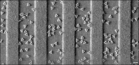 |
| Triangular "DNA origami" were made to assemble on etched carbon and silicon |
Abstract:
Today, scientists at IBM (NYSE: IBM) Research and the California Institute of Technology announced a scientific advancement that could be a major breakthrough in enabling the semiconductor industry to pack more power and speed into tiny computer chips, while making them more energy efficient and less expensive to manufacture.
IBM Scientists Use DNA Scaffolding To Build Tiny Circuit Boards: Nanotechnology advancement could lead to smaller, faster, more energy efficient computer chips
San Jose, CA | Posted on August 17th, 2009IBM researchers and collaborator Paul W.K. Rothemund, of the California Institute of Technology, have made an advancement in combining lithographic patterning with self assembly - a method to arrange DNA origami structures on surfaces compatible with today's semiconductor manufacturing equipment.
Today, the semiconductor industry is faced with the challenges of developing lithographic technology for feature sizes smaller than 22 nm and exploring new classes of transistors that employ carbon nanotubes or silicon nanowires. IBM's approach of using DNA molecules as scaffolding -- where millions of carbon nanotubes could be deposited and self-assembled into precise patterns by sticking to the DNA molecules - may provide a way to reach sub-22 nm lithography.
The utility of this approach lies in the fact that the positioned DNA nanostructures can serve as scaffolds, or miniature circuit boards, for the precise assembly of components - such as carbon nanotubes, nanowires and nanoparticles - at dimensions significantly smaller than possible with conventional semiconductor fabrication techniques. This opens up the possibility of creating functional devices that can be integrated into larger structures, as well as enabling studies of arrays of nanostructures with known coordinates.
"The cost involved in shrinking features to improve performance is a limiting factor in keeping pace with Moore's Law and a concern across the semiconductor industry," said Spike Narayan, manager, Science & Technology, IBM Research - Almaden. "The combination of this directed self-assembly with today's fabrication technology eventually could lead to substantial savings in the most expensive and challenging part of the chip-making process."
The techniques for preparing DNA origami, developed at Caltech, cause single DNA molecules to self assemble in solution via a reaction between a long single strand of viral DNA and a mixture of different short synthetic oligonucleotide strands. These short segments act as staples - effectively folding the viral DNA into the desired 2D shape through complementary base pair binding. The short staples can be modified to provide attachment sites for nanoscale components at resolutions (separation between sites) as small as 6 nanometers (nm). In this way, DNA nanostructures such as squares, triangles and stars can be prepared with dimensions of 100 - 150 nm on an edge and a thickness of the width of the DNA double helix.
The lithographic templates were fabricated at IBM using traditional semiconductor techniques, the same used to make the chips found in today's computers, to etch out patterns. Either electron beam or optical lithography were used to create arrays of binding sites of the proper size and shape to match those of individual origami structures. Key to the process were the discovery of the template material and deposition conditions to afford high selectivity so that origami binds only to the patterns of "sticky patches" and nowhere else.
The paper on this work, "Placement and orientation of DNA nanostructures on lithographically patterned surfaces," by scientists at IBM Research and the California Institute of Technology, will be published in the September issue of Nature Nanotechnology and is currently available at: http://www.nature.com/nnano/journal/vaop/ncurrent/abs/nnano.2009.220.html.
####
For more information, please click here
Contacts:
Research & Development
Emerging technologies
Jenny Galitz McTighe
Media Relations director
914-945-1016
Mobile phone: 917-499-8123
Copyright © IBM
If you have a comment, please Contact us.Issuers of news releases, not 7th Wave, Inc. or Nanotechnology Now, are solely responsible for the accuracy of the content.
Bookmark:


| Related News Press |
News and information
![]() Simulating magnetization in a Heisenberg quantum spin chain April 5th, 2024
Simulating magnetization in a Heisenberg quantum spin chain April 5th, 2024
![]() NRL charters Navy�s quantum inertial navigation path to reduce drift April 5th, 2024
NRL charters Navy�s quantum inertial navigation path to reduce drift April 5th, 2024
![]() Discovery points path to flash-like memory for storing qubits: Rice find could hasten development of nonvolatile quantum memory April 5th, 2024
Discovery points path to flash-like memory for storing qubits: Rice find could hasten development of nonvolatile quantum memory April 5th, 2024
Chip Technology
![]() Discovery points path to flash-like memory for storing qubits: Rice find could hasten development of nonvolatile quantum memory April 5th, 2024
Discovery points path to flash-like memory for storing qubits: Rice find could hasten development of nonvolatile quantum memory April 5th, 2024
![]() Utilizing palladium for addressing contact issues of buried oxide thin film transistors April 5th, 2024
Utilizing palladium for addressing contact issues of buried oxide thin film transistors April 5th, 2024
![]() HKUST researchers develop new integration technique for efficient coupling of III-V and silicon February 16th, 2024
HKUST researchers develop new integration technique for efficient coupling of III-V and silicon February 16th, 2024
Nanoelectronics
![]() Interdisciplinary: Rice team tackles the future of semiconductors Multiferroics could be the key to ultralow-energy computing October 6th, 2023
Interdisciplinary: Rice team tackles the future of semiconductors Multiferroics could be the key to ultralow-energy computing October 6th, 2023
![]() Key element for a scalable quantum computer: Physicists from Forschungszentrum J�lich and RWTH Aachen University demonstrate electron transport on a quantum chip September 23rd, 2022
Key element for a scalable quantum computer: Physicists from Forschungszentrum J�lich and RWTH Aachen University demonstrate electron transport on a quantum chip September 23rd, 2022
![]() Reduced power consumption in semiconductor devices September 23rd, 2022
Reduced power consumption in semiconductor devices September 23rd, 2022
![]() Atomic level deposition to extend Moore�s law and beyond July 15th, 2022
Atomic level deposition to extend Moore�s law and beyond July 15th, 2022
Discoveries
![]() Chemical reactions can scramble quantum information as well as black holes April 5th, 2024
Chemical reactions can scramble quantum information as well as black holes April 5th, 2024
![]() New micromaterial releases nanoparticles that selectively destroy cancer cells April 5th, 2024
New micromaterial releases nanoparticles that selectively destroy cancer cells April 5th, 2024
![]() Utilizing palladium for addressing contact issues of buried oxide thin film transistors April 5th, 2024
Utilizing palladium for addressing contact issues of buried oxide thin film transistors April 5th, 2024
Announcements
![]() NRL charters Navy�s quantum inertial navigation path to reduce drift April 5th, 2024
NRL charters Navy�s quantum inertial navigation path to reduce drift April 5th, 2024
![]() Discovery points path to flash-like memory for storing qubits: Rice find could hasten development of nonvolatile quantum memory April 5th, 2024
Discovery points path to flash-like memory for storing qubits: Rice find could hasten development of nonvolatile quantum memory April 5th, 2024
|
|
||
|
|
||
| The latest news from around the world, FREE | ||
|
|
||
|
|
||
| Premium Products | ||
|
|
||
|
Only the news you want to read!
Learn More |
||
|
|
||
|
Full-service, expert consulting
Learn More |
||
|
|
||