Home > Press > The future is 3-D liquid crystals
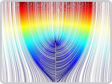 |
| Simulation of the electric field surrounding a single MWCNT in vacuum. |
Abstract:
Simulation of the electric field surrounding a single MWCNT in vacuum.Dr Tim Wilkinson from the Cambridge University Department of Engineering's Photonics Research Group has made an exciting breakthrough. He has combined liquid crystals with vertically grown carbon nanotubes to create a reconfigurable three-dimensional liquid crystal device structure.
The future is 3-D liquid crystals
Cambridge, UK | Posted on January 15th, 2009This offers completely new ways to control molecules in liquid crystals, allowing the crystals to move in a variety of directions to create optical components such as lenslet arrays. This technology is still in the early phase of development, but recent trials indicate that potential applications exist in adaptive optical systems such as the wavefront sensors used in optometry, digital video cameras, optical diffusers and emerging head-up display devices.
Liquid crystal (LC) molecules are shaped so that they naturally align with each other if put in a cell to form an optically active pixel. In a display device the liquid crystal pixel is used to change the polarisation of the light passing through it and the degree of change (seen as contrast) is done through an applied voltage onto electrodes at the top and bottom of the cell. The applied voltage makes the LC molecules rotate in the cell and changes their orientation with respect to the light passing through the cell. This cell geometry limits the ways in which the light can interact with the liquid crystal molecules to a 2 dimensional plane. If we add a 3 dimensional element to the lower electrode we can change the way in which the voltage interact with the LC molecules to make a 3 dimensional optical structure. A simple example is shown on the top image on the right handside, where a thin conducting rod is added to the lower electrode to create a Gaussian electric field profile which forms a tiny microlens in the LC material. With many rods it is possible to create array of micro lenses which can have a focal length that varies with the applied voltage. Such a reconfigurable array has many uses in adaptive optical systems and 3D holographic displays.
Talking about his work, Tim says: "My idea is to combine two well established technologies, liquid crystals and nanotechnology to make a new hybrid device. The LCs has the ability to create a reconfigurable optical modulator (such as would be seen as 2D pixels in a liquid crystal device (LCD)) with the vertically grown multiwall carbon nanotubes (MWCNT) which act as a 3D electrode structure. In a traditional LC device (such as a display screen) the pixel electrodes are above and below the LC and allow it to be switched in a simple way. In the hybrid device the lower electrode is the MWCNT grown on silicon which sticks out from the surface into the 3rd dimension. This is also a more complex electric field profile which in turn creates a more complicated 3D refractive index profile in the LC layer. Hence we can make very complicated optical elements using a very simple device structure and an applied voltage to switch it.
"An example is when the MWCNTs on the lower electrode surface are all connected and switched with the same voltage. The resulting electric field profile surrounding each MWCNT electrode is Gaussian in shape which creates a Gaussian refractive index profile in the LC layer. This looks optically like a tiny lens which is centred on each MWCNT, hence for an array of CNTs spaced 10μm apart we end up with an array of microlenses 10μm apart. By changing the voltage applied to the CNTs we can switch the micro lenses on and off and also vary their focal length. There are many applications for such a switchable microlens array such as in adaptive optical systems where the ability to self focus a lens is important or as an active diffuser in a head mounted display system.
"More importantly this breakthrough changes the way in which we think about creating liquid crystal devices. It allows us to include a 3D element to the design of modulating characteristics. If we address each individual CNT with a separate voltage then we can build more complex 3D refractive index profiles similar to those you would see in a full 3D photographically recorded hologram. However the difference with the LC/CNT device is that the hologram can be changed dynamically as you would change an image on a LCD. This allows full 3D displays to be built using this sort of technology."
Articles on this research appeared in EuroPhotonics trade magazine (August 2008), in Advanced Materials and in Advanced Imaging Magazine (January 2009).
####
For more information, please click here
Copyright © University of Cambridge
If you have a comment, please Contact us.Issuers of news releases, not 7th Wave, Inc. or Nanotechnology Now, are solely responsible for the accuracy of the content.
Bookmark:


| Related News Press |
News and information
![]() Quantum computer improves AI predictions April 17th, 2026
Quantum computer improves AI predictions April 17th, 2026
![]() Flexible sensor gains sensitivity under pressure April 17th, 2026
Flexible sensor gains sensitivity under pressure April 17th, 2026
![]() A reusable chip for particulate matter sensing April 17th, 2026
A reusable chip for particulate matter sensing April 17th, 2026
![]() Detecting vibrational quantum beating in the predissociation dynamics of SF6 using time-resolved photoelectron spectroscopy April 17th, 2026
Detecting vibrational quantum beating in the predissociation dynamics of SF6 using time-resolved photoelectron spectroscopy April 17th, 2026
Display technology/LEDs/SS Lighting/OLEDs
![]() Spinel-type sulfide semiconductors to operate the next-generation LEDs and solar cells For solar-cell absorbers and green-LED source October 3rd, 2025
Spinel-type sulfide semiconductors to operate the next-generation LEDs and solar cells For solar-cell absorbers and green-LED source October 3rd, 2025
![]() Efficient and stable hybrid perovskite-organic light-emitting diodes with external quantum efficiency exceeding 40 per cent July 5th, 2024
Efficient and stable hybrid perovskite-organic light-emitting diodes with external quantum efficiency exceeding 40 per cent July 5th, 2024
Nanotubes/Buckyballs/Fullerenes/Nanorods/Nanostrings/Nanosheets
![]() Tiny nanosheets, big leap: A new sensor detects ethanol at ultra-low levels January 30th, 2026
Tiny nanosheets, big leap: A new sensor detects ethanol at ultra-low levels January 30th, 2026
![]() Enhancing power factor of p- and n-type single-walled carbon nanotubes April 25th, 2025
Enhancing power factor of p- and n-type single-walled carbon nanotubes April 25th, 2025
![]() Chainmail-like material could be the future of armor: First 2D mechanically interlocked polymer exhibits exceptional flexibility and strength January 17th, 2025
Chainmail-like material could be the future of armor: First 2D mechanically interlocked polymer exhibits exceptional flexibility and strength January 17th, 2025
![]() Innovative biomimetic superhydrophobic coating combines repair and buffering properties for superior anti-erosion December 13th, 2024
Innovative biomimetic superhydrophobic coating combines repair and buffering properties for superior anti-erosion December 13th, 2024
Discoveries
![]() Quantum computer improves AI predictions April 17th, 2026
Quantum computer improves AI predictions April 17th, 2026
![]() Flexible sensor gains sensitivity under pressure April 17th, 2026
Flexible sensor gains sensitivity under pressure April 17th, 2026
![]() A reusable chip for particulate matter sensing April 17th, 2026
A reusable chip for particulate matter sensing April 17th, 2026
![]() Detecting vibrational quantum beating in the predissociation dynamics of SF6 using time-resolved photoelectron spectroscopy April 17th, 2026
Detecting vibrational quantum beating in the predissociation dynamics of SF6 using time-resolved photoelectron spectroscopy April 17th, 2026
Announcements
![]() A fundamentally new therapeutic approach to cystic fibrosis: Nanobody repairs cellular defect April 17th, 2026
A fundamentally new therapeutic approach to cystic fibrosis: Nanobody repairs cellular defect April 17th, 2026
![]() UC Irvine physicists discover method to reverse �quantum scrambling� : The work addresses the problem of information loss in quantum computing system April 17th, 2026
UC Irvine physicists discover method to reverse �quantum scrambling� : The work addresses the problem of information loss in quantum computing system April 17th, 2026
|
|
||
|
|
||
| The latest news from around the world, FREE | ||
|
|
||
|
|
||
| Premium Products | ||
|
|
||
|
Only the news you want to read!
Learn More |
||
|
|
||
|
Full-service, expert consulting
Learn More |
||
|
|
||