Home > Press > Northeastern University Physicists Create Assembly Technique for Carbon Nanotubes
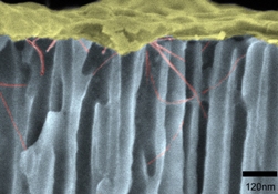 |
| A cross-sectional view of SEM micrographs of assembled SWNTs in anodic alumina array fabricated on Silican |
Abstract:
Srinivas Sridhar, Ph.D., distinguished professor and chair of Physics at Northeastern University, Evin Gultepe and their team of researchers from the university's Electronic Materials Research Institute have demonstrated a technique to assemble single-walled carbon nanotubes (SWNT) into three-dimensional structures. This technique will be useful for the large scale, accelerated assembly of SWNTs at room temperature, which is more suitable for nanoscale electronic applications, such as flat panel displays and electronic memory devices.
Northeastern University Physicists Create Assembly Technique for Carbon Nanotubes
Boston, MA | Posted on October 29th, 2008This research was published in an October 2008 issue of the journal Nanotechnology.
The electronic properties of SWNTs, such as large current capacities and quick mobility, makes them one of the most highly researched structures for the development of nanoscale electronics. They are able to conduct energy more quickly and efficiently than current structures and provide a platform from which to build smaller-scale products. Widely used materials, such as copper, do not meet the requirements as effective electrical interconnects on a smaller scale.
The challenge of utilizing carbon nanotubes (CNT) in the nanoscale is to assemble them into three-dimensional structures for large scale applications. Currently, manufacturing CNTs requires growing or assembling them into a device, which requires very hot temperatures and complex post-assembly procedures. In contrast, a post-synthesis assembly method allows for the arrangement of CNTs in ambient temperatures, which gives more flexibility in the manufacturing process.
In this newly discovered process, Gultepe, Sridhar and their colleagues manufactured nanotemplates, with billions of nano-sized holes in which to house the SWNTs. Utilizing electrical fields, they were able assemble the SWNTs vertically into the alumina nanotemplate, with a silican substrate bottom layer and a metal top layer. The vertically-assembled three-dimensional SWNTs provide the electrical interconnection between the nanotemplates and the silicon substrates.
"The greatest significance of this process is the potential to manufacture three-dimensional SWNTs electrical interconnects at a high-rate and on a larger scale," said Sridhar, who is also the Director of the Electronic Materials Research Institute at Northeastern. "Scaling down the nominal feature size means greater performance and decreased costs."
In addition to Sridhar, the team of researches involved with this project includes Ahmed Busnaina, Ph.D., Director of Northeastern's Center for High-rate Nanomanufacturing, Dattatri Nagesha, Ph.D., Bernard Diddier Frederic Casse, Ph.D., and Selvapraba Selvarasah. This research was supported by the IGERT Nanomedicine Science and Technology and the NSF Nanoscale Science and Engineering Centers Program.
####
About Northeastern University
Founded in 1898, Northeastern University is a private research university located in the heart of Boston. Northeastern is a leader in interdisciplinary research, urban engagement, and the integration of classroom learning with real-world experience. The university�s distinctive cooperative education program, where students alternate semesters of full-time study with semesters of paid work in fields relevant to their professional interests and major, is one of the largest and most innovative in the world. The University offers a comprehensive range of undergraduate and graduate programs leading to degrees through the doctorate in six undergraduate colleges, eight graduate schools, and two part-time divisions.
For more information, please click here
Contacts:
Jenny Eriksen
(617) 373-2802
Copyright © Northeastern University
If you have a comment, please Contact us.Issuers of news releases, not 7th Wave, Inc. or Nanotechnology Now, are solely responsible for the accuracy of the content.
Bookmark:


| Related News Press |
News and information
![]() Simulating magnetization in a Heisenberg quantum spin chain April 5th, 2024
Simulating magnetization in a Heisenberg quantum spin chain April 5th, 2024
![]() NRL charters Navy�s quantum inertial navigation path to reduce drift April 5th, 2024
NRL charters Navy�s quantum inertial navigation path to reduce drift April 5th, 2024
![]() Discovery points path to flash-like memory for storing qubits: Rice find could hasten development of nonvolatile quantum memory April 5th, 2024
Discovery points path to flash-like memory for storing qubits: Rice find could hasten development of nonvolatile quantum memory April 5th, 2024
![]() Good as gold - improving infectious disease testing with gold nanoparticles April 5th, 2024
Good as gold - improving infectious disease testing with gold nanoparticles April 5th, 2024
Display technology/LEDs/SS Lighting/OLEDs
![]() Utilizing palladium for addressing contact issues of buried oxide thin film transistors April 5th, 2024
Utilizing palladium for addressing contact issues of buried oxide thin film transistors April 5th, 2024
![]() Light guide plate based on perovskite nanocomposites November 3rd, 2023
Light guide plate based on perovskite nanocomposites November 3rd, 2023
![]() Simple ballpoint pen can write custom LEDs August 11th, 2023
Simple ballpoint pen can write custom LEDs August 11th, 2023
Memory Technology
![]() Utilizing palladium for addressing contact issues of buried oxide thin film transistors April 5th, 2024
Utilizing palladium for addressing contact issues of buried oxide thin film transistors April 5th, 2024
![]() Interdisciplinary: Rice team tackles the future of semiconductors Multiferroics could be the key to ultralow-energy computing October 6th, 2023
Interdisciplinary: Rice team tackles the future of semiconductors Multiferroics could be the key to ultralow-energy computing October 6th, 2023
![]() Researchers discover materials exhibiting huge magnetoresistance June 9th, 2023
Researchers discover materials exhibiting huge magnetoresistance June 9th, 2023
Nanotubes/Buckyballs/Fullerenes/Nanorods/Nanostrings
![]() Tests find no free-standing nanotubes released from tire tread wear September 8th, 2023
Tests find no free-standing nanotubes released from tire tread wear September 8th, 2023
![]() Detection of bacteria and viruses with fluorescent nanotubes July 21st, 2023
Detection of bacteria and viruses with fluorescent nanotubes July 21st, 2023
Discoveries
![]() Chemical reactions can scramble quantum information as well as black holes April 5th, 2024
Chemical reactions can scramble quantum information as well as black holes April 5th, 2024
![]() New micromaterial releases nanoparticles that selectively destroy cancer cells April 5th, 2024
New micromaterial releases nanoparticles that selectively destroy cancer cells April 5th, 2024
![]() Utilizing palladium for addressing contact issues of buried oxide thin film transistors April 5th, 2024
Utilizing palladium for addressing contact issues of buried oxide thin film transistors April 5th, 2024
Announcements
![]() NRL charters Navy�s quantum inertial navigation path to reduce drift April 5th, 2024
NRL charters Navy�s quantum inertial navigation path to reduce drift April 5th, 2024
![]() Discovery points path to flash-like memory for storing qubits: Rice find could hasten development of nonvolatile quantum memory April 5th, 2024
Discovery points path to flash-like memory for storing qubits: Rice find could hasten development of nonvolatile quantum memory April 5th, 2024
|
|
||
|
|
||
| The latest news from around the world, FREE | ||
|
|
||
|
|
||
| Premium Products | ||
|
|
||
|
Only the news you want to read!
Learn More |
||
|
|
||
|
Full-service, expert consulting
Learn More |
||
|
|
||