Home > Press > Scientists grow 'nanonets' able to snare added energy transfer
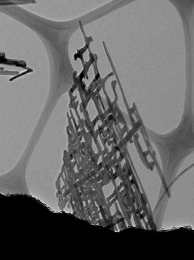 |
| Researchers at Boston College report creating nanonets, pictured here magnified 50,000 times. The novel nano-scale structure was grown from titanium and silicon in a two-dimensional network of wires that resembles flat, rectangular netting.
Credit: Angewandte Chemie International |
Abstract:
New structure improves material used in microelectronics and water-splitting
Scientists grow 'nanonets' able to snare added energy transfer
CHESTNUT HILL, MA | Posted on September 2nd, 2008Using two abundant and relatively inexpensive elements, Boston College chemists have produced nanonets, a flexible webbing of nano-scale wires that multiplies surface area critical to improving the performance of the wires in electronics and energy applications.
Researchers grew wires from titanium and silicon into a two-dimensional network of branches that resemble flat, rectangular netting, Assistant Professor of Chemistry Professor Dunwei Wang and his team report in the international edition of the German Chemical Society journal Angewandte Chemie.
By creating nanonets, the team conquered a longstanding engineering challenge in nanotechnology: creating a material that is extremely thin yet maintains its complexity, a structural design large or long enough to efficiently transfer an electrical charge.
"We wanted to create a nano structure unlike any other with a relatively large surface area," said Wang. "The goal was to increase surface area and maintain the structural integrity of the material without sacrificing surface area and thereby improving performance."
Tests showed an improved performance in the material's ability to conduct electricity through high quality connections of the nanonet, which suggest the material could lend itself to applications from electronics to energy-harvesting, Wang said. Titanium disilicide (TiSi2) has been proven to absorb light across a wide range of the solar spectrum, is easily obtained, and is inexpensive. Metal silicides are also found in microelectronics devices.
The nanonets grew spontaneously from the bottom-up through simple chemical reactions, unprovoked by a catalyst, according to Wang and co-authors, post doctoral researcher Xiaohua Liu and graduate students Sa Zhou and Yongjing Lin.
Basic nano structures are commonly created in zero or one dimension, such as a dot composed of a small number of atoms. The most complex structures grow in three dimensions - somewhat resembling the branches of a tree. Working in 2D, Wang's team produced a web that under a microscope resembles a tree with all branches growing in the same perpendicular direction from the trunk.
Using titanium disilicide intrigued Wang because of the material's superior conductivity. Late last year, researchers at the Max Planck Institute for Bioinorganic Chemistry observed that a titanium disilicide semiconductor photo catalyst splits water into hydrogen and oxygen. The semiconductor also stores the gases produced, enabling the simple separation of hydrogen and oxygen. So-called water splitting may play a key role in producing hydrogen for fuel.
"We're excited to have discovered this unique structure and we are already at work to gauge just how much the nanonet can improve the performance of a material that is already used in electronics and clean energy applications," said Wang.
The full paper can be viewed at
www3.interscience.wiley.com/cgi-bin/fulltext/121393485/PDFSTART
For more information about Prof. Wang's lab, please visit the website: www2.bc.edu/~dwang/
####
For more information, please click here
Contacts:
Ed Hayward
617-552-4826
Copyright © Boston College
If you have a comment, please Contact us.Issuers of news releases, not 7th Wave, Inc. or Nanotechnology Now, are solely responsible for the accuracy of the content.
Bookmark:


| Related News Press |
News and information
![]() Simulating magnetization in a Heisenberg quantum spin chain April 5th, 2024
Simulating magnetization in a Heisenberg quantum spin chain April 5th, 2024
![]() NRL charters Navy�s quantum inertial navigation path to reduce drift April 5th, 2024
NRL charters Navy�s quantum inertial navigation path to reduce drift April 5th, 2024
![]() Discovery points path to flash-like memory for storing qubits: Rice find could hasten development of nonvolatile quantum memory April 5th, 2024
Discovery points path to flash-like memory for storing qubits: Rice find could hasten development of nonvolatile quantum memory April 5th, 2024
Nanoelectronics
![]() Interdisciplinary: Rice team tackles the future of semiconductors Multiferroics could be the key to ultralow-energy computing October 6th, 2023
Interdisciplinary: Rice team tackles the future of semiconductors Multiferroics could be the key to ultralow-energy computing October 6th, 2023
![]() Key element for a scalable quantum computer: Physicists from Forschungszentrum J�lich and RWTH Aachen University demonstrate electron transport on a quantum chip September 23rd, 2022
Key element for a scalable quantum computer: Physicists from Forschungszentrum J�lich and RWTH Aachen University demonstrate electron transport on a quantum chip September 23rd, 2022
![]() Reduced power consumption in semiconductor devices September 23rd, 2022
Reduced power consumption in semiconductor devices September 23rd, 2022
![]() Atomic level deposition to extend Moore�s law and beyond July 15th, 2022
Atomic level deposition to extend Moore�s law and beyond July 15th, 2022
Discoveries
![]() Chemical reactions can scramble quantum information as well as black holes April 5th, 2024
Chemical reactions can scramble quantum information as well as black holes April 5th, 2024
![]() New micromaterial releases nanoparticles that selectively destroy cancer cells April 5th, 2024
New micromaterial releases nanoparticles that selectively destroy cancer cells April 5th, 2024
![]() Utilizing palladium for addressing contact issues of buried oxide thin film transistors April 5th, 2024
Utilizing palladium for addressing contact issues of buried oxide thin film transistors April 5th, 2024
Announcements
![]() NRL charters Navy�s quantum inertial navigation path to reduce drift April 5th, 2024
NRL charters Navy�s quantum inertial navigation path to reduce drift April 5th, 2024
![]() Discovery points path to flash-like memory for storing qubits: Rice find could hasten development of nonvolatile quantum memory April 5th, 2024
Discovery points path to flash-like memory for storing qubits: Rice find could hasten development of nonvolatile quantum memory April 5th, 2024
Energy
![]() Development of zinc oxide nanopagoda array photoelectrode: photoelectrochemical water-splitting hydrogen production January 12th, 2024
Development of zinc oxide nanopagoda array photoelectrode: photoelectrochemical water-splitting hydrogen production January 12th, 2024
![]() Shedding light on unique conduction mechanisms in a new type of perovskite oxide November 17th, 2023
Shedding light on unique conduction mechanisms in a new type of perovskite oxide November 17th, 2023
![]() Inverted perovskite solar cell breaks 25% efficiency record: Researchers improve cell efficiency using a combination of molecules to address different November 17th, 2023
Inverted perovskite solar cell breaks 25% efficiency record: Researchers improve cell efficiency using a combination of molecules to address different November 17th, 2023
![]() The efficient perovskite cells with a structured anti-reflective layer � another step towards commercialization on a wider scale October 6th, 2023
The efficient perovskite cells with a structured anti-reflective layer � another step towards commercialization on a wider scale October 6th, 2023
|
|
||
|
|
||
| The latest news from around the world, FREE | ||
|
|
||
|
|
||
| Premium Products | ||
|
|
||
|
Only the news you want to read!
Learn More |
||
|
|
||
|
Full-service, expert consulting
Learn More |
||
|
|
||