Home > Press > Northwestern Chemists Take Gold, Mass-Produce Beijing Olympic Logo
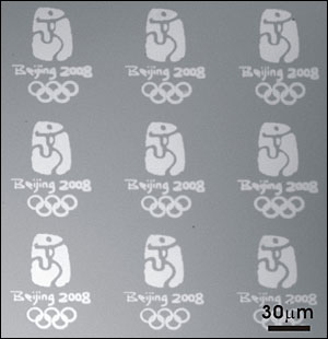 |
| Each Olympic logo is so small � 70 micrometers long and 60 micrometers wide � that 2,500 of them would fit on a grain of rice. |
Abstract:
Northwestern University nanoscientist Chad A. Mirkin has mass-produced the 2008 Summer Olympics logo -- 15,000 times. All the logos take up only one square centimeter of space.
Northwestern Chemists Take Gold, Mass-Produce Beijing Olympic Logo
EVANSTON, IL | Posted on August 14th, 2008Mirkin and his colleagues printed the logos as well as an integrated gold circuit using a new printing technique, called Polymer Pen Lithography (PPL), that can write on three different length scales using only one device.
The PPL technique, to be published Aug. 15 in Science Express, is a fast, inexpensive and simple way to print on the nanometer, micrometer and millimeter length scales.
The new printing method could find use in computational tools (the electronics that make up these tools), medical diagnostics (gene chips and arrays of biomolecules) and the pharmaceutical industry (arrays for screening drug candidates), among others.
"While watching the Olympics opening night ceremonies I was delighted to see that printing was highlighted as one of ancient China's four great inventions," said Mirkin, George B. Rathmann Professor of Chemistry in the Weinberg College of Arts and Sciences, professor of medicine and professor of materials science and engineering. Mirkin led the study.
"We consider Dip-Pen Nanolithography, which is nanotechnology's version of the quill pen, and now Polymer Pen Lithography to be two of Northwestern's most important inventions."
Polymer Pen Lithography uses arrays of tiny pens made of polymers to print over large areas with nanoscopic through macroscopic resolution. By simply changing contact pressure (and the amount the pens deform), as well as the time of delivery, dots of various diameters can be produced. (The pen tips snap back to their original shape when the pressure is removed.)
"We can go, in a sense, from an ultra fine point Sharpie� to one with a fat tip," said Mirkin, director of Northwestern's International Institute for Nanotechnology. "The tip of each polymer pen starts with nanometer-scale sharpness, but if we press down harder the tip flattens out. This gives us great flexibility in the structures we can produce."
In the case of the Olympic logo, the researchers started with a bitmap image of the logo and uniformly printed 15,000 replicas onto a gold substrate using an "ink" of the molecule 16-mercaptohexadecanoic acid. (The ink is a mere one molecule thick.) This took less than 40 minutes.
The logo is so small that 2,500 of them would fit on a single grain of rice. The letters and numbers, "Beijing 2008," were generated from approximately 20,000 dots that were 90 nanometers in diameter. Then, with more force applied to the pens, the stylized human figure and the Olympic rings were made from approximately 4,000 dots that were 600 nanometers in diameter.
The integrated circuit the researchers built had features on all three length scales, perfectly integrated together. Building the circuit took about two hours. As with the Olympic logo, the structures were made by making multiple printing passes with the same tool (the pen array, which has an ink reservoir).
Polymer Pen Lithography simplifies and takes the best of two existing printing techniques -- the high registration and sub-50-nanometer resolution of Dip-Pen Nanolithography (DPN) and the use of a polymer stamp to transfer a pattern in microcontact printing. (Mirkin invented DPN in 1999.)
The PPL method requires a dot matrix image of the structure to be printed (the Olympic logo, for example) and an atomic force microscope. The researchers have demonstrated arrays with as many as 11 million pens.
The Science paper is titled "Polymer Pen Lithography." In addition to Mirkin, other authors are Fengwei Huo (lead author), Zijian Zheng, Gengfeng Zheng, Louise R. Giam and Hua Zhang, all of Northwestern.
The research was supported by the Air Force Office of Scientific Research, the Defense Advanced Research Projects Agency and the National Science Foundation.
####
For more information, please click here
Contacts:
Megan Fellman
847-491-3115
Copyright © Northwestern University
If you have a comment, please Contact us.Issuers of news releases, not 7th Wave, Inc. or Nanotechnology Now, are solely responsible for the accuracy of the content.
Bookmark:


| Related News Press |
News and information
![]() Simulating magnetization in a Heisenberg quantum spin chain April 5th, 2024
Simulating magnetization in a Heisenberg quantum spin chain April 5th, 2024
![]() NRL charters Navy�s quantum inertial navigation path to reduce drift April 5th, 2024
NRL charters Navy�s quantum inertial navigation path to reduce drift April 5th, 2024
![]() Discovery points path to flash-like memory for storing qubits: Rice find could hasten development of nonvolatile quantum memory April 5th, 2024
Discovery points path to flash-like memory for storing qubits: Rice find could hasten development of nonvolatile quantum memory April 5th, 2024
Chip Technology
![]() Discovery points path to flash-like memory for storing qubits: Rice find could hasten development of nonvolatile quantum memory April 5th, 2024
Discovery points path to flash-like memory for storing qubits: Rice find could hasten development of nonvolatile quantum memory April 5th, 2024
![]() Utilizing palladium for addressing contact issues of buried oxide thin film transistors April 5th, 2024
Utilizing palladium for addressing contact issues of buried oxide thin film transistors April 5th, 2024
![]() HKUST researchers develop new integration technique for efficient coupling of III-V and silicon February 16th, 2024
HKUST researchers develop new integration technique for efficient coupling of III-V and silicon February 16th, 2024
Announcements
![]() NRL charters Navy�s quantum inertial navigation path to reduce drift April 5th, 2024
NRL charters Navy�s quantum inertial navigation path to reduce drift April 5th, 2024
![]() Discovery points path to flash-like memory for storing qubits: Rice find could hasten development of nonvolatile quantum memory April 5th, 2024
Discovery points path to flash-like memory for storing qubits: Rice find could hasten development of nonvolatile quantum memory April 5th, 2024
Sports
![]() Surrey reveals its implantable biosensor that operates without batteries May 22nd, 2020
Surrey reveals its implantable biosensor that operates without batteries May 22nd, 2020
![]() Collagen nanofibrils in mammalian tissues get stronger with exercise December 14th, 2018
Collagen nanofibrils in mammalian tissues get stronger with exercise December 14th, 2018
![]() Epoxy compound gets a graphene bump: Rice scientists combine graphene foam, epoxy into tough, conductive composite November 14th, 2018
Epoxy compound gets a graphene bump: Rice scientists combine graphene foam, epoxy into tough, conductive composite November 14th, 2018
Human Interest/Art
![]() Drawing data in nanometer scale September 30th, 2022
Drawing data in nanometer scale September 30th, 2022
![]() Scientists prepare for the world�s smallest race: Nanocar Race II March 18th, 2022
Scientists prepare for the world�s smallest race: Nanocar Race II March 18th, 2022
![]() Graphene nanotubes revolutionize touch screen use for prosthetic hands August 3rd, 2021
Graphene nanotubes revolutionize touch screen use for prosthetic hands August 3rd, 2021
![]() JEOL Announces 2020 Microscopy Image Grand Prize Winners January 7th, 2021
JEOL Announces 2020 Microscopy Image Grand Prize Winners January 7th, 2021
Printing/Lithography/Inkjet/Inks/Bio-printing/Dyes
![]() Presenting: Ultrasound-based printing of 3D materials�potentially inside the body December 8th, 2023
Presenting: Ultrasound-based printing of 3D materials�potentially inside the body December 8th, 2023
![]() Simple ballpoint pen can write custom LEDs August 11th, 2023
Simple ballpoint pen can write custom LEDs August 11th, 2023
![]() Disposable electronics on a simple sheet of paper October 7th, 2022
Disposable electronics on a simple sheet of paper October 7th, 2022
|
|
||
|
|
||
| The latest news from around the world, FREE | ||
|
|
||
|
|
||
| Premium Products | ||
|
|
||
|
Only the news you want to read!
Learn More |
||
|
|
||
|
Full-service, expert consulting
Learn More |
||
|
|
||