Home > Press > Exposing the Sensitivity of Extreme Ultraviolet Photoresists
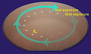 |
| NIST researchers exposed a 300 mm silicon wafer with incrementally increasing doses of extreme ultraviolet light (EUV) in 15 areas. After the wafer was developed, the team determined that the seventh exposure was the minimum dose required (E0) to fully remove the resist.
Credit: NIST |
Abstract:
Researchers at the National Institute of Standards and Technology (NIST) have confirmed that the photoresists used in next-generation semiconductor manufacturing processes now under development are twice as sensitive as previously believed. This finding, announced at a workshop last month,* has attracted considerable interest because of its implications for future manufacturing. If the photoresists are twice as sensitive as previously thought, then they are close to having the sensitivity required for high volume manufacturing, but the flip side is that the extreme ultraviolet optical systems in the demonstration tools currently being used are only about half as effective as believed.
Exposing the Sensitivity of Extreme Ultraviolet Photoresists
GAITHERSBURG, MD | Posted on June 26th, 2008Extreme ultraviolet lithography (EUVL) is a process analogous to film photography. A silicon wafer is coated with photoresist and exposed to EUV light that reflects off a patterned "photomask." Where the light strikes the resist it changes the solubility of the coating. When developed, the soluble portions wash away leaving the same pattern exposed on the silicon surface for the processing steps that ultimately create microcircuits.
The drive to make circuits with ever smaller features has pushed manufacturers to use shorter and shorter wavelengths of light. EUVL is the next step in this progression and requires developing both suitable light sources and photoresists that can retain the fine details of the circuit, balancing sensitivity, line edge roughness and spatial resolution. NIST researcher Steve Grantham says that optical lithography light sources in use today emit light with a wavelength of about 193 nanometers, which borders on optical wavelengths. EUVL sources produce light with wavelengths about an order of magnitude smaller, around 13.5 nanometers. Because this light does not travel through anything�including lenses�mirrors have to be used to focus it.
Until recently, EUV photoresist sensitivity was referenced to a measurement technique developed at Sandia National Labs in the 1990s. Late in 2007, scientists at the Advanced Light Source at Lawrence Berkeley National Laboratory in Berkeley, Calif., used a NIST-calibrated photodetector to check the standard. Their detector-based measurements indicated that the resist's sensitivity was about twice that of the resist-based calibration standard.
Following on the intense interest that these results generated when the Berkeley group presented them at a conference in February, the Intel Corporation asked scientists at NIST to make their own independent determination of the EUVL resist sensitivity to validate the results. Measurements conducted at the NIST SURF III Synchrotron Ultraviolet Radiation Facility agreed with those of the Berkeley group. The fact that the photoresist is now known to be twice as sensitive to the EUV light implies that half as much light energy as had been expected is arriving at the wafer.
"These results are significant for a technology that faces many challenges before it is slated to become a high-volume manufacturing process in 2012," Grantham says. "It should open the eyes of the industry to the need for accurate dose metrology and the use of traceable standards in their evaluations of source and lithography tool performance."
* S. Grantham, C. Tarrio, R. E. Vest, T. B. Lucatorto, A. Novembre, M. Cangemi, V. Prabhu, K.W. Choi, M. Chandhok, T. Younkin and J. S. Clarke. SEMATECH EUV Source Workshop, Bolton Landing, N.Y., May 12, 2008.
####
About NIST
Founded in 1901, NIST is a non-regulatory federal agency within the U.S. Department of Commerce. NIST's mission is to promote U.S. innovation and industrial competitiveness by advancing measurement science, standards, and technology in ways that enhance economic security and improve our quality of life.
For more information, please click here
Contacts:
Mark Esser
(301) 975-8735
Copyright © NIST
If you have a comment, please Contact us.Issuers of news releases, not 7th Wave, Inc. or Nanotechnology Now, are solely responsible for the accuracy of the content.
Bookmark:


| Related News Press |
News and information
![]() Simulating magnetization in a Heisenberg quantum spin chain April 5th, 2024
Simulating magnetization in a Heisenberg quantum spin chain April 5th, 2024
![]() NRL charters Navy�s quantum inertial navigation path to reduce drift April 5th, 2024
NRL charters Navy�s quantum inertial navigation path to reduce drift April 5th, 2024
![]() Discovery points path to flash-like memory for storing qubits: Rice find could hasten development of nonvolatile quantum memory April 5th, 2024
Discovery points path to flash-like memory for storing qubits: Rice find could hasten development of nonvolatile quantum memory April 5th, 2024
Chip Technology
![]() Discovery points path to flash-like memory for storing qubits: Rice find could hasten development of nonvolatile quantum memory April 5th, 2024
Discovery points path to flash-like memory for storing qubits: Rice find could hasten development of nonvolatile quantum memory April 5th, 2024
![]() Utilizing palladium for addressing contact issues of buried oxide thin film transistors April 5th, 2024
Utilizing palladium for addressing contact issues of buried oxide thin film transistors April 5th, 2024
![]() HKUST researchers develop new integration technique for efficient coupling of III-V and silicon February 16th, 2024
HKUST researchers develop new integration technique for efficient coupling of III-V and silicon February 16th, 2024
Nanoelectronics
![]() Interdisciplinary: Rice team tackles the future of semiconductors Multiferroics could be the key to ultralow-energy computing October 6th, 2023
Interdisciplinary: Rice team tackles the future of semiconductors Multiferroics could be the key to ultralow-energy computing October 6th, 2023
![]() Key element for a scalable quantum computer: Physicists from Forschungszentrum J�lich and RWTH Aachen University demonstrate electron transport on a quantum chip September 23rd, 2022
Key element for a scalable quantum computer: Physicists from Forschungszentrum J�lich and RWTH Aachen University demonstrate electron transport on a quantum chip September 23rd, 2022
![]() Reduced power consumption in semiconductor devices September 23rd, 2022
Reduced power consumption in semiconductor devices September 23rd, 2022
![]() Atomic level deposition to extend Moore�s law and beyond July 15th, 2022
Atomic level deposition to extend Moore�s law and beyond July 15th, 2022
Discoveries
![]() Chemical reactions can scramble quantum information as well as black holes April 5th, 2024
Chemical reactions can scramble quantum information as well as black holes April 5th, 2024
![]() New micromaterial releases nanoparticles that selectively destroy cancer cells April 5th, 2024
New micromaterial releases nanoparticles that selectively destroy cancer cells April 5th, 2024
![]() Utilizing palladium for addressing contact issues of buried oxide thin film transistors April 5th, 2024
Utilizing palladium for addressing contact issues of buried oxide thin film transistors April 5th, 2024
Announcements
![]() NRL charters Navy�s quantum inertial navigation path to reduce drift April 5th, 2024
NRL charters Navy�s quantum inertial navigation path to reduce drift April 5th, 2024
![]() Discovery points path to flash-like memory for storing qubits: Rice find could hasten development of nonvolatile quantum memory April 5th, 2024
Discovery points path to flash-like memory for storing qubits: Rice find could hasten development of nonvolatile quantum memory April 5th, 2024
Photonics/Optics/Lasers
![]() With VECSELs towards the quantum internet Fraunhofer: IAF achieves record output power with VECSEL for quantum frequency converters April 5th, 2024
With VECSELs towards the quantum internet Fraunhofer: IAF achieves record output power with VECSEL for quantum frequency converters April 5th, 2024
![]() Nanoscale CL thermometry with lanthanide-doped heavy-metal oxide in TEM March 8th, 2024
Nanoscale CL thermometry with lanthanide-doped heavy-metal oxide in TEM March 8th, 2024
![]() Optically trapped quantum droplets of light can bind together to form macroscopic complexes March 8th, 2024
Optically trapped quantum droplets of light can bind together to form macroscopic complexes March 8th, 2024
![]() HKUST researchers develop new integration technique for efficient coupling of III-V and silicon February 16th, 2024
HKUST researchers develop new integration technique for efficient coupling of III-V and silicon February 16th, 2024
|
|
||
|
|
||
| The latest news from around the world, FREE | ||
|
|
||
|
|
||
| Premium Products | ||
|
|
||
|
Only the news you want to read!
Learn More |
||
|
|
||
|
Full-service, expert consulting
Learn More |
||
|
|
||