Home > Press > High Performance Transistors Created with Carbon 60
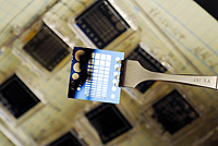 |
| Georgia Tech researchers have fabricated high-performance field effect transistors with thin films of Carbon 60, also known as fullerene. |
Abstract:
Devices mark another milestone toward producing low-cost circuits on flexible substrates
High Performance Transistors Created with Carbon 60
Atlanta, GA | Posted on November 26th, 2007Using room-temperature processing, researchers at the Georgia Institute of Technology have fabricated high-performance field effect transistors with thin films of Carbon 60, also known as fullerene. The ability to produce devices with such performance with an organic semiconductor represents another milestone toward practical applications for large area, low-cost electronic circuits on flexible organic substrates.
The new devices - which have electron-mobility values higher than amorphous silicon, low threshold voltages, large on-off ratios and high operational stability - could encourage more designers to begin working on such circuitry for displays, active electronic billboards, RFID tags and other applications that use flexible substrates.
"If you open a textbook and look at what a thin-film transistor should do, we are pretty close now," said Bernard Kippelen, a professor in Georgia Tech's School of Electrical and Computer Engineering and the Center for Organic Photonics and Electronics. "Now that we have shown very nice single transistors, we want to demonstrate functional devices that are combinations of multiple components. We have everything ready to do that."
Fabrication of the C60 transistors was reported August 27 in the journal Applied Physics Letters. The research was supported by the U.S. National Science Foundation through the STC program MDITR, and the U.S. Office of Naval Research.
Researchers have been interested in making field-effect transistors and other devices from organic semiconductors that can be processed onto various substrates, including flexible plastic materials. As an organic semiconductor material, C60 is attractive because it can provide high electron mobility - a measure of how fast current can flow. Previous reports have shown that C60 can yield mobility values as high as six square centimeters per volt-second (6 cm2/V/s).
However, that record was achieved using a hot-wall epitaxy process requiring processing temperatures of 250 degrees Celsius - too hot for most flexible plastic substrates.
Though the transistors produced by Kippelen's research team display slightly lower electron mobility - 2.7 to 5 cm2/V/s - they can be produced at room temperature.
"If you want to deposit transistors on a plastic substrate, you really can't have any process at a temperature of more than 150 degrees Celsius," Kippelen said. "With room temperature deposition, you can be compatible with many different substrates. For low-cost, large area electronics, that is an essential component."
Because they are sensitive to contact with oxygen, the C60 transistors must operate under a nitrogen atmosphere. Kippelen expects to address that limitation by using other fullerene molecules - and properly packaging the devices.
The new transistors were fabricated on silicon for convenience. While Kippelen isn't underestimating the potential difficulty of moving to an organic substrate, he says that challenge can be overcome.
Though their performance is impressive, the C60 transistors won't threaten conventional CMOS chips based on silicon. That's because the applications Kippelen has in mind don't require high performance.
"There are a lot of applications where you don't necessarily need millions of fast transistors," he said. "The performance we need is by far much lower than what you can get in a CMOS chip. But whereas CMOS is extremely powerful and can be relatively low in cost because you can make a lot of circuits on a wafer, for large area applications CMOS is not economical."
A different set of goals drives electronic components for use with low-cost organic displays, active billboards and similar applications.
"If you look at a video display, which has a refresh rate of 60 Hz, than means you have to refresh the screen every 16 milliseconds," he noted. "That is a fairly low speed compared to a Pentium processor in your computer. There is no point in trying to use organic materials for high-speed processing because silicon is already very advanced and has much higher carrier mobility."
Now that they have demonstrated attractive field-effect C60 transistors, Kippelen and collaborators Xiao-Hong Zhang and Benoit Domercq plan to produce other electronic components such as inverters, ring oscillators, logic gates, and drivers for active matrix displays and imaging devices. Assembling these more complex systems will showcase the advantages of the C60 devices.
"The goal is to increase the complexity of the circuits to see how that high mobility can be used to make more complex structures with unprecedented performance," Kippelen said.
The researchers fabricated the transistors by depositing C60 molecules from the vapor phase into a thin film atop a silicon substrate onto which a gate electrode and gate dielectric had already been fabricated. The source and drain electrodes were then deposited on top of the C60 films through a shadow mask.
Kippelen's team has been working with C60 for nearly ten years, and is also using the material in photovoltaic cells. Beyond the technical advance, Kippelen believes this new work demonstrates the growing maturity of organic electronics.
"This progress may trigger interest among more conventional electronic engineers," he said. "Most engineers would like to work with the latest technology platform, but they would like to see a level of performance showing they could actually implement these circuits. If you can demonstrate - as we have - that you can get transistors with good reproducibility, good stability, near-zero threshold voltages, large on-off current ratios and performance levels higher than amorphous silicon, that may convince designers to consider this technology."
####
About Georgia Tech
The Georgia Institute of Technology is one of the nation's premiere research universities. Ranked seventh among U.S. News & World Report's top public universities, Georgia Tech's more than 18,000 students are enrolled in its Colleges of Architecture, Computing, Engineering, Liberal Arts, Management and Sciences. Tech is among the nation's top producers of women and African-American engineers. The Institute offers research opportunities to both undergraduate and graduate students and is home to more than 100 interdisciplinary units plus the Georgia Tech Research Institute.
For more information, please click here
Contacts:
John Toon
Research News & Publications Office
404-894-6986
Abby Vogel
404-385-3364
Technical Contact:
Bernard Kippelen
404-385-5163
Copyright © Georgia Tech
If you have a comment, please Contact us.Issuers of news releases, not 7th Wave, Inc. or Nanotechnology Now, are solely responsible for the accuracy of the content.
Bookmark:


| Related Links |
![]() Center for Organic Photonics and Electronics
Center for Organic Photonics and Electronics
![]() School of Electrical and Computer Engineering
School of Electrical and Computer Engineering
| Related News Press |
Chip Technology
![]() A reusable chip for particulate matter sensing April 17th, 2026
A reusable chip for particulate matter sensing April 17th, 2026
![]() Metasurfaces smooth light to boost magnetic sensing precision January 30th, 2026
Metasurfaces smooth light to boost magnetic sensing precision January 30th, 2026
Nanoelectronics
![]() Lab to industry: InSe wafer-scale breakthrough for future electronics August 8th, 2025
Lab to industry: InSe wafer-scale breakthrough for future electronics August 8th, 2025
![]() Interdisciplinary: Rice team tackles the future of semiconductors Multiferroics could be the key to ultralow-energy computing October 6th, 2023
Interdisciplinary: Rice team tackles the future of semiconductors Multiferroics could be the key to ultralow-energy computing October 6th, 2023
![]() Key element for a scalable quantum computer: Physicists from Forschungszentrum J�lich and RWTH Aachen University demonstrate electron transport on a quantum chip September 23rd, 2022
Key element for a scalable quantum computer: Physicists from Forschungszentrum J�lich and RWTH Aachen University demonstrate electron transport on a quantum chip September 23rd, 2022
![]() Reduced power consumption in semiconductor devices September 23rd, 2022
Reduced power consumption in semiconductor devices September 23rd, 2022
Discoveries
![]() Quantum computer improves AI predictions April 17th, 2026
Quantum computer improves AI predictions April 17th, 2026
![]() Flexible sensor gains sensitivity under pressure April 17th, 2026
Flexible sensor gains sensitivity under pressure April 17th, 2026
![]() A reusable chip for particulate matter sensing April 17th, 2026
A reusable chip for particulate matter sensing April 17th, 2026
![]() Detecting vibrational quantum beating in the predissociation dynamics of SF6 using time-resolved photoelectron spectroscopy April 17th, 2026
Detecting vibrational quantum beating in the predissociation dynamics of SF6 using time-resolved photoelectron spectroscopy April 17th, 2026
Announcements
![]() A fundamentally new therapeutic approach to cystic fibrosis: Nanobody repairs cellular defect April 17th, 2026
A fundamentally new therapeutic approach to cystic fibrosis: Nanobody repairs cellular defect April 17th, 2026
![]() UC Irvine physicists discover method to reverse �quantum scrambling� : The work addresses the problem of information loss in quantum computing system April 17th, 2026
UC Irvine physicists discover method to reverse �quantum scrambling� : The work addresses the problem of information loss in quantum computing system April 17th, 2026
RFID
![]() Nanowire 'inks' enable paper-based printable electronics: Highly conductive films make functional circuits without adding high heat January 4th, 2017
Nanowire 'inks' enable paper-based printable electronics: Highly conductive films make functional circuits without adding high heat January 4th, 2017
![]() Conformal transfer of graphene for reproducible device fabrication August 11th, 2015
Conformal transfer of graphene for reproducible device fabrication August 11th, 2015
|
|
||
|
|
||
| The latest news from around the world, FREE | ||
|
|
||
|
|
||
| Premium Products | ||
|
|
||
|
Only the news you want to read!
Learn More |
||
|
|
||
|
Full-service, expert consulting
Learn More |
||
|
|
||