Home > Press > Breakthrough toward industrial-scale production of nanodevices
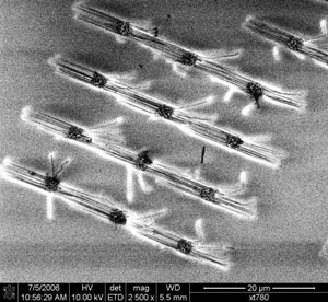 |
| Researchers in Maryland report an advance toward making zinc oxide nanowires (shown) on an industrial scale. Courtesy of Babak Nikoobakht, National Institute of Standards and Technology |
Abstract:
Scientists in Maryland are reporting an important advance toward the long-sought goal of industrial-scale fabrication of nanowire-based devices like ultra-sensitive sensors, light emitting diodes, and transistors for inexpensive, high-performance electronics products. The study is scheduled for the current issue of ACS' Chemistry of Materials, a bi-weekly journal.
Breakthrough toward industrial-scale production of nanodevices
Gaithersburg, MD | Posted on November 7th, 2007In the report, Babak Nikoobakht points out that existing state-of-the-art assembly methods for nanowire-based devices require complicated, multi-step treatments, painstaking alignments steps, and other processing for nanowires , which are thousands of times smaller than the diameter of a human hair. The goal is to electrically address the coordinates of millions of nanowires on a surface in order to produce the components of electronic circuits.
The study describes a new method in which zinc oxide nanowires are grown in the exact positions where nanodevices later will be fabricated, in a way that involves a minimum number of fabrication steps and is suitable for industrial-scale applications. "This method, due to its scalability and ease of device fabrication, goes beyond the current state-of-the-art assembly of nanowire-based devices," the report states. "It is believed to be an attractive approach for mass fabrication of nanowire-based transistors and sensors and is expected to impact nanotechnology in fabrication of nonconventional nanodevices."
####
About American Chemical Society
The American Chemical Society � the world's largest scientific society � is a nonprofit organization chartered by the U.S. Congress and a global leader in providing access to chemistry-related research through its multiple databases, peer-reviewed journals and scientific conferences. Its main offices are in Washington, D.C., and Columbus, Ohio.
For more information, please click here
Contacts:
Babak Nikoobakht, Ph.D.
National Institute of Standards and Technology
Gaithersburg, Maryland 20899
Phone: 301-975-3230
Fax: 301- 926-6689
Email:
Copyright © American Chemical Society
If you have a comment, please Contact us.Issuers of news releases, not 7th Wave, Inc. or Nanotechnology Now, are solely responsible for the accuracy of the content.
Bookmark:


| Related Links |
| Related News Press |
Chip Technology
![]() Discovery points path to flash-like memory for storing qubits: Rice find could hasten development of nonvolatile quantum memory April 5th, 2024
Discovery points path to flash-like memory for storing qubits: Rice find could hasten development of nonvolatile quantum memory April 5th, 2024
![]() Utilizing palladium for addressing contact issues of buried oxide thin film transistors April 5th, 2024
Utilizing palladium for addressing contact issues of buried oxide thin film transistors April 5th, 2024
![]() HKUST researchers develop new integration technique for efficient coupling of III-V and silicon February 16th, 2024
HKUST researchers develop new integration technique for efficient coupling of III-V and silicon February 16th, 2024
Nanoelectronics
![]() Interdisciplinary: Rice team tackles the future of semiconductors Multiferroics could be the key to ultralow-energy computing October 6th, 2023
Interdisciplinary: Rice team tackles the future of semiconductors Multiferroics could be the key to ultralow-energy computing October 6th, 2023
![]() Key element for a scalable quantum computer: Physicists from Forschungszentrum J�lich and RWTH Aachen University demonstrate electron transport on a quantum chip September 23rd, 2022
Key element for a scalable quantum computer: Physicists from Forschungszentrum J�lich and RWTH Aachen University demonstrate electron transport on a quantum chip September 23rd, 2022
![]() Reduced power consumption in semiconductor devices September 23rd, 2022
Reduced power consumption in semiconductor devices September 23rd, 2022
![]() Atomic level deposition to extend Moore�s law and beyond July 15th, 2022
Atomic level deposition to extend Moore�s law and beyond July 15th, 2022
Discoveries
![]() Chemical reactions can scramble quantum information as well as black holes April 5th, 2024
Chemical reactions can scramble quantum information as well as black holes April 5th, 2024
![]() New micromaterial releases nanoparticles that selectively destroy cancer cells April 5th, 2024
New micromaterial releases nanoparticles that selectively destroy cancer cells April 5th, 2024
![]() Utilizing palladium for addressing contact issues of buried oxide thin film transistors April 5th, 2024
Utilizing palladium for addressing contact issues of buried oxide thin film transistors April 5th, 2024
Announcements
![]() NRL charters Navy�s quantum inertial navigation path to reduce drift April 5th, 2024
NRL charters Navy�s quantum inertial navigation path to reduce drift April 5th, 2024
![]() Discovery points path to flash-like memory for storing qubits: Rice find could hasten development of nonvolatile quantum memory April 5th, 2024
Discovery points path to flash-like memory for storing qubits: Rice find could hasten development of nonvolatile quantum memory April 5th, 2024
|
|
||
|
|
||
| The latest news from around the world, FREE | ||
|
|
||
|
|
||
| Premium Products | ||
|
|
||
|
Only the news you want to read!
Learn More |
||
|
|
||
|
Full-service, expert consulting
Learn More |
||
|
|
||