Home > Press > NIST Demos Industrial-Grade Nanowire Device Fabrication
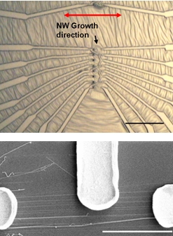 |
| Nanowire electronics: (Top) Optical image shows metal electrodes attached to zinc oxide nanowires using the NIST technique. Dark spots near the center are the gold pads that start nanowire growth; red arrow shows direction of growth. Scale bar is 50 micrometers long. (Bottom) Scanning electron microscope image shows electrodes connected to group of nanowires. Scale bar is five micrometers long.
Credit: NIST |
Abstract:
In the growing catalog of nanoscale technologies, nanowires—tiny rows of conductor or semiconductor atoms—have attracted a great deal of interest for their potential to build unique atomic-scale electronics. But before you can buy some at your local Nano Depot, manufacturers will need efficient, reliable methods to build them in quantity. Researchers at the National Institute of Standards and Technology (NIST) believe they have one solution—a technique that allows them to selectively grow nanowires on sapphire wafers in specific positions and orientations accurately enough to attach contacts and layer other circuit elements, all with conventional lithography techniques. They detailed their results in a recent paper.*
NIST Demos Industrial-Grade Nanowire Device Fabrication
GAITHERSBURG, MD | Posted on November 1st, 2007Despite their name, nanowires are more than just electrical connectors. Researchers have used nanowires to create transistors like those used in memory devices and prototype sensors for gases or biomolecules. However working with objects only tens of nanometers wide is challenging. A common approach in the lab is to grow nanowires like blades of grass on a suitable substrate, mow them off and mix them in a fluid to transfer them to a test surface, using some method to give them a preferred orientation. When the carrier fluid dries, the nanowires are left behind like tumbled jackstraws. Using scanning probe microscopy or similar tools, researchers hunt around for a convenient, isolated nanowire to work on, or place electrical contacts without knowing the exact positions of the nanowires. It's not a technique suitable for mass production.
Building on earlier work to grow nanowires horizontally on the surface of wafers (see "Gold Nano Anchors Put Nanowires in Their Place"), NIST researchers used conventional semiconductor manufacturing techniques to deposit small amounts of gold in precise locations on a sapphire wafer. In a high-temperature process, the gold deposits bead up into nanodroplets that act as nucleation points for crystals of zinc oxide, a semiconductor. A slight mismatch in the crystal structures of zinc oxide and sapphire induces the semiconductor to grow as a narrow nanowire in one particular direction across the wafer. Because the starting points and the growth direction are both well known, it is relatively straightforward to add electrical contacts and other features with additional lithography steps.
As proof of concept, the NIST researchers have used this procedure to create more than 600 nanowire-based transistors, a circuit element commonly used in digital memory chips, in a single process. In the prototype process, they report, the nanowires typical grew in small bunches of up to eight wires at a time, but finer control over the size of the initial gold deposits should make it possible to select the number of wires in each position. The technique, they say, should allow industrial-scale production of nanowire-based devices.
For more examples of NIST research on nanowire electronics, see: "New Design Developed for Silicon Nanowire Transistors," "Growing Glowing Nanowires to Light Up the Nanoworld," "New Fabrication Technique Yields Nanoscale UV LEDs," "Placing Single Nanowires: NIST Makes the Connection," and "Silicon Nanowires Upgrade Data-Storage Technology."
* B. Nikoobakht. Toward industrial-scale fabrication of nanowire-based devices. Chem. Mater., ASAP Article 10.1021/cm071798p S0897-4756(07)01798-X. Web Release Date: October 9, 2007.
####
About NIST
NIST, an agency of the U.S. Department of Commerce, was founded in 1901 as the nation's first federal physical science research laboratory. Over the years, the scientists and technical staff at NIST have made solid contributions to image processing, DNA diagnostic "chips," smoke detectors, and automated error-correcting software for machine tools. Just a few of the other areas in which NIST has had major impact include atomic clocks, X-ray standards for mammography, scanning tunneling microscopy, pollution-control technology, and high-speed dental drills. We invite you to explore our web site to learn about our current projects, to find out how you can work with us, or to make use of our products and services.
For more information, please click here
Contacts:
Michael Baum
(301) 975-2763
Copyright © NIST
If you have a comment, please Contact us.Issuers of news releases, not 7th Wave, Inc. or Nanotechnology Now, are solely responsible for the accuracy of the content.
Bookmark:


| Related News Press |
Nanoelectronics
![]() Interdisciplinary: Rice team tackles the future of semiconductors Multiferroics could be the key to ultralow-energy computing October 6th, 2023
Interdisciplinary: Rice team tackles the future of semiconductors Multiferroics could be the key to ultralow-energy computing October 6th, 2023
![]() Key element for a scalable quantum computer: Physicists from Forschungszentrum Jülich and RWTH Aachen University demonstrate electron transport on a quantum chip September 23rd, 2022
Key element for a scalable quantum computer: Physicists from Forschungszentrum Jülich and RWTH Aachen University demonstrate electron transport on a quantum chip September 23rd, 2022
![]() Reduced power consumption in semiconductor devices September 23rd, 2022
Reduced power consumption in semiconductor devices September 23rd, 2022
![]() Atomic level deposition to extend Moore’s law and beyond July 15th, 2022
Atomic level deposition to extend Moore’s law and beyond July 15th, 2022
Discoveries
![]() Chemical reactions can scramble quantum information as well as black holes April 5th, 2024
Chemical reactions can scramble quantum information as well as black holes April 5th, 2024
![]() New micromaterial releases nanoparticles that selectively destroy cancer cells April 5th, 2024
New micromaterial releases nanoparticles that selectively destroy cancer cells April 5th, 2024
![]() Utilizing palladium for addressing contact issues of buried oxide thin film transistors April 5th, 2024
Utilizing palladium for addressing contact issues of buried oxide thin film transistors April 5th, 2024
Announcements
![]() NRL charters Navy’s quantum inertial navigation path to reduce drift April 5th, 2024
NRL charters Navy’s quantum inertial navigation path to reduce drift April 5th, 2024
![]() Discovery points path to flash-like memory for storing qubits: Rice find could hasten development of nonvolatile quantum memory April 5th, 2024
Discovery points path to flash-like memory for storing qubits: Rice find could hasten development of nonvolatile quantum memory April 5th, 2024
|
|
||
|
|
||
| The latest news from around the world, FREE | ||
|
|
||
|
|
||
| Premium Products | ||
|
|
||
|
Only the news you want to read!
Learn More |
||
|
|
||
|
Full-service, expert consulting
Learn More |
||
|
|
||