Home > Press > Park Systems Launches Park NX20 300mm Research Atomic Force Microscope with Full 300 mm Semiconductor Wafer Scan - Vastly Improving Productivity
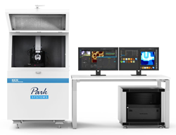 |
| Park NX20 300mm - first research AFM on the market capable of scanning the entire sample area of 300 mm wafers using a 300 mm vacuum chuck while keeping the system noise level below 0.5angst |
Abstract:
Park Systems, world leading manufacturer of Atomic Force Microscopes (AFM) today announced Park NX20 300mm, the first and only research AFM on the market capable of scanning the entire sample area of 300 mm wafers using a 300 mm vacuum chuck while keeping the system noise level below 0.5angstrom (Ĺ) RMS. The automated measurements over a 300 mm wafer dramatically improve user-convenience and productivity in the industrial lab setting where comparisons within site-to-site and sample-to-sample surface morphologies (height, surface roughness measurements) are extremely important.
Park Systems Launches Park NX20 300mm Research Atomic Force Microscope with Full 300 mm Semiconductor Wafer Scan - Vastly Improving Productivity
Santa Clara, CA | Posted on August 3rd, 2016“Today large samples of up to 300 mm wafers and substrates are widely used for process development, failure analysis, and production but so far there has not been an AFM measurement tool that can accurately measure the full area in one load, and easily program it to take multiple site measurements in one click,” comments Keibock Lee, Park Systems President. “Park NX20 300mm accesses the entire 300 mm wafer in a single loading with low-noise AFM measurements, which opens up a whole new scope of measurement automation on a 300 mm wafer.”
Park NX20 300mm enables AFM inspection and scans over the entire sample area of 300 mm wafers by using a full 300 mm x 300 mm motorized XY stage so the system can access any location on a 300 mm wafer. Park’s NX20 300 mm is the only product that can hold a 300 mm sample unlike current products on the market, for example the competitor’s system that come closest to Park is combined with 300 mm sample chuck but requires the user to load 9 times to access the entire 300 mm wafer area because the range of the motorized XY stage is limited to 180 mm x 220 mm.
Park NX20 300mm standard vacuum chuck is designed to hold samples ranging in size from 300 mm to 100 mm, and can even support small coupon samples of arbitrary shapes using a vacuum hole. Products on the market now are limited to 200 mm sample sizes and must rely on cutting up the sample to maintain the low noise required by industry, which is cumbersome and makes sharing the AFM challenging. The new Park NX20 is the perfect solution for shared labs whose samples come in various sizes--small and large—as it supports from large to small coupon samples and is compatible with all the modes and options available to Park's other research AFM products.
Park Systems, recognized for innovation in Nanoscale metrology, is the recipient of the Frost and Sullivan 2016 Global Enabling Technology Leadership Award for Its proprietary technologies, such as the SmartScan OS and True Non-Contact Mode which have given its products an edge over competing solutions in terms of user friendliness, efficiency, and accuracy. These innovations have allowed Park Systems to bring the power of AFM to a wider user-base, enabling researchers and engineers further scientific discoveries and technological progress from materials to semiconductor to life sciences.
“Park NX20 300mm is another demonstration of Park Systems’s ability to innovate products demanded in today’s fast-growing semiconductor industry where status quo will not suffice in this new era of nanotechnology advances,” states Frost & Sullivan Industry Analyst Mariano Kimbara.
Since 1997, Park Systems has added significant innovations to their original AFM design to revolutionize imaging methodologies and enhance the user experience, resulting in their unbridled success. Park Systems holds 32 patents related to AFM technology, including True Non-Contact Mode™ using decoupled XY and Z scanners, PTR measurements of HDD application, NX-Bio technology using Scanning ion conductance microscopy (SICM) on live cell, 3D AFM, Full automation AFM operation software (SmartScan™). SmartScan fully automatizes AFM imaging making it very easy for anyone to take an image of a sample at nanoscale resolution and clarity comparable to one taken by an expert.
Park Systems has a full range of AFM systems that provide solutions for researchers and industry engineers across a wide spectrum of disciplines including chemistry, materials, physics, life sciences, semiconductor and data storage. Used by thousands of the most distinguished academic and research institutions worldwide, Park is recognized as an innovate partner in nanoscale technologies.
####
About Park Systems
Park Systems is a world-leading manufacturer of atomic force microscopy (AFM) systems with a complete range of products for researchers and industry engineers in chemistry, materials, physics, life sciences, semiconductor and data storage industries. Park’s products are used by over a thousand of institutions and corporations worldwide. Park’s AFM provides highest data accuracy at nanoscale resolution, superior productivity, and lowest operating cost thanks to its unique technology and innovative engineering. Park Systems, Inc. is headquartered in Santa Clara, California with its global manufacturing, and R&D headquarters in Korea. Park’s products are sold and supported worldwide with regional headquarters in the US, Korea, Japan, and Singapore, and distribution partners throughout Europe, Asia, and America. Please visit http://www.parkafm.com or call 408-986-1110 for more information.
For more information, please click here
Contacts:
Gerald Pascual
408-986-1110
Copyright © Park Systems
If you have a comment, please Contact us.Issuers of news releases, not 7th Wave, Inc. or Nanotechnology Now, are solely responsible for the accuracy of the content.
Bookmark:


| Related News Press |
News and information
![]() Quantum computer improves AI predictions April 17th, 2026
Quantum computer improves AI predictions April 17th, 2026
![]() Flexible sensor gains sensitivity under pressure April 17th, 2026
Flexible sensor gains sensitivity under pressure April 17th, 2026
![]() A reusable chip for particulate matter sensing April 17th, 2026
A reusable chip for particulate matter sensing April 17th, 2026
![]() Detecting vibrational quantum beating in the predissociation dynamics of SF6 using time-resolved photoelectron spectroscopy April 17th, 2026
Detecting vibrational quantum beating in the predissociation dynamics of SF6 using time-resolved photoelectron spectroscopy April 17th, 2026
Imaging
![]() Simple algorithm paired with standard imaging tool could predict failure in lithium metal batteries August 8th, 2025
Simple algorithm paired with standard imaging tool could predict failure in lithium metal batteries August 8th, 2025
Software
![]() Visualizing nanoscale structures in real time: Open-source software enables researchers to see materials in 3D while they're still on the electron microscope August 19th, 2022
Visualizing nanoscale structures in real time: Open-source software enables researchers to see materials in 3D while they're still on the electron microscope August 19th, 2022
![]() Luisier wins SNSF Advanced Grant to develop simulation tools for nanoscale devices July 8th, 2022
Luisier wins SNSF Advanced Grant to develop simulation tools for nanoscale devices July 8th, 2022
![]() Oxford Instruments’ Atomfab® system is production-qualified at a market-leading GaN power electronics device manufacturer December 17th, 2021
Oxford Instruments’ Atomfab® system is production-qualified at a market-leading GaN power electronics device manufacturer December 17th, 2021
Announcements
![]() A fundamentally new therapeutic approach to cystic fibrosis: Nanobody repairs cellular defect April 17th, 2026
A fundamentally new therapeutic approach to cystic fibrosis: Nanobody repairs cellular defect April 17th, 2026
![]() UC Irvine physicists discover method to reverse ‘quantum scrambling’ : The work addresses the problem of information loss in quantum computing system April 17th, 2026
UC Irvine physicists discover method to reverse ‘quantum scrambling’ : The work addresses the problem of information loss in quantum computing system April 17th, 2026
Tools
![]() Metasurfaces smooth light to boost magnetic sensing precision January 30th, 2026
Metasurfaces smooth light to boost magnetic sensing precision January 30th, 2026
![]() From sensors to smart systems: the rise of AI-driven photonic noses January 30th, 2026
From sensors to smart systems: the rise of AI-driven photonic noses January 30th, 2026
![]() Japan launches fully domestically produced quantum computer: Expo visitors to experience quantum computing firsthand August 8th, 2025
Japan launches fully domestically produced quantum computer: Expo visitors to experience quantum computing firsthand August 8th, 2025
|
|
||
|
|
||
| The latest news from around the world, FREE | ||
|
|
||
|
|
||
| Premium Products | ||
|
|
||
|
Only the news you want to read!
Learn More |
||
|
|
||
|
Full-service, expert consulting
Learn More |
||
|
|
||