Home > Press > Nanocrystals Not Small Enough to Avoid Defects: Berkeley Lab Scientists at Advanced Light Source Show Dislocations Can Be Induced by Pressure in Ultrafine Nanocrystals
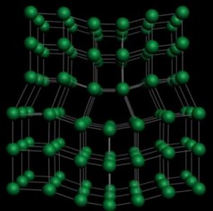 |
| Stress-induced deformation of nanocrystalline nickel reflects the dislocation activity observed by researchers at Berkeley Lab�s Advanced Light Source using a radial diamond-anvil-cell X-ray diffraction experimental station. (Image courtesy of NDT Education Resource Center) |
Abstract:
Nanocrystals as protective coatings for advanced gas turbine and jet engines are receiving a lot of attention for their many advantageous mechanical properties, including their resistance to stress. However, contrary to computer simulations, the tiny size of nanocrystals apparently does not safeguard them from defects.
Nanocrystals Not Small Enough to Avoid Defects: Berkeley Lab Scientists at Advanced Light Source Show Dislocations Can Be Induced by Pressure in Ultrafine Nanocrystals
Berkeley, CA | Posted on December 14th, 2012In a study by researchers with the U.S. Department of Energy (DOE)'s Lawrence Berkeley National Laboratory (Berkeley Lab)and collaborators from multiple institutions, nanocrystals of nickel subjected to high pressure continued to suffer dislocation-mediated plastic deformation even when the crystals were only three nanometers in size. These experimental findings, which were carried out at Berkeley Lab's Advanced Light Source (ALS), a premier source of X-rays and ultraviolet light for scientific research, show that dislocations can form in the finest of nanocrystals when stress is applied.
"We cannot ignore or underestimate the role of dislocations - defects or irregularities - in fine nanocrystals as external stress can change the entire picture," says Bin Chen, a materials scientist with the ALS Experimental Systems Group who led this research. "Our results demonstrate that dislocation-mediated deformation persists to smaller crystal sizes than anticipated, primarily because computer models have not given enough consideration to the effects of external stress and grain boundaries."
Chen is the lead and corresponding author of a paper in Science describing this work. The paper is titled "Texture of Nanocrystalline Nickel: Probing the Lower Size Limit of Dislocation Activity." Co-authoring this paper were Katie Lutker, Selva Vennila Raju, Jinyuan Yan, Waruntorn Kanitpanyacharoen, Jialin Lei, Shizhong Yang, Hans-Rudolf Wenk, Ho-kwang Mao and Quentin Williams.
Plastic deformation is a permanent change in the shape or size of a material as the result of an applied stress. The likelihood of plastic deformation increases with the presence of dislocations - defects or irregularities - within the material's structure. Most materials are made up of small crystals, called "grains," and what happens at the boundaries between these grains is critical to material properties. Based on computer simulations and electron microscopy analysis, the belief has been that dislocation-mediated plastic deformation becomes inactive below a grain size of at least 10 nanometers, and possibly as large as 30 nanometers.
"The idea was that below a critical length scale, dislocation-mediated deformation activity would give way to grain-boundary sliding, diffusion, and grain rotation," Chen says. "However, there were many unresolved questions with regards to whether plasticity in ultrafine nanocrystalline grains could still be generated by dislocations and how pressure might affect the deformational regimes."
To investigate grain size and pressure effects on the plastic deformation of nanometals, Chen and his colleagues used ALS Beamline 12.2.2, a superconducting bend magnet beamline that supports radial diamond-anvil-cell X-ray diffraction experiments. Chen and his co-authors recorded in situ observations under a range of high pressures of texturing (when the crystalline grains have preferred orientations) in stressed polycrystalline nickel samples featuring grain sizes of 500-, 20- and 3-nanometers.
"Substantial texturing was observed at pressures above 3.0 gigapascals for nickel with 500-nanometer grain size and at greater than 11.0 gigapascals for nickel with 20-nanometer grain size," Chen says. "Surprisingly, texturing was also seen in nickel with 3-nanometer grain size when compressed above 18.5 gigapascals. This tells us that under high external pressures, dislocation activity can be extended down to a few-nanometers-length scale."
Chen and his co-authors started with nanocrystalline nickel because its face-center cubic structure remains stable under a wide pressure range. They are now applying their techniques to the study of other nanocrystalline materials, both metals and non-metals.
This research was funded by the National Science Foundation, NASA and the DOE Office of Science. The ALS is a DOE Office of Science national user facility.
####
About DOE/Lawrence Berkeley National Laboratory
Lawrence Berkeley National Laboratory addresses the world�s most urgent scientific challenges by advancing sustainable energy, protecting human health, creating new materials, and revealing the origin and fate of the universe. Founded in 1931, Berkeley Lab�s scientific expertise has been recognized with 13 Nobel prizes. The University of California manages Berkeley Lab for the U.S. Department of Energy�s Office of Science. For more, visit www.lbl.gov.
DOE�s Office of Science is the single largest supporter of basic research in the physical sciences in the United States, and is working to address some of the most pressing challenges of our time. For more information, please visit the Office of Science website at science.energy.gov/.
For more information, please click here
Contacts:
Lynn Yarris
510-486-5375
Copyright © Berkeley Lab
If you have a comment, please Contact us.Issuers of news releases, not 7th Wave, Inc. or Nanotechnology Now, are solely responsible for the accuracy of the content.
Bookmark:


| Related Links |
![]() For more about the Advanced Light Source go here:
For more about the Advanced Light Source go here:
| Related News Press |
News and information
![]() Quantum computer improves AI predictions April 17th, 2026
Quantum computer improves AI predictions April 17th, 2026
![]() Flexible sensor gains sensitivity under pressure April 17th, 2026
Flexible sensor gains sensitivity under pressure April 17th, 2026
![]() A reusable chip for particulate matter sensing April 17th, 2026
A reusable chip for particulate matter sensing April 17th, 2026
![]() Detecting vibrational quantum beating in the predissociation dynamics of SF6 using time-resolved photoelectron spectroscopy April 17th, 2026
Detecting vibrational quantum beating in the predissociation dynamics of SF6 using time-resolved photoelectron spectroscopy April 17th, 2026
Laboratories
![]() Researchers develop molecular qubits that communicate at telecom frequencies October 3rd, 2025
Researchers develop molecular qubits that communicate at telecom frequencies October 3rd, 2025
![]() A battery�s hopping ions remember where they�ve been: Seen in atomic detail, the seemingly smooth flow of ions through a battery�s electrolyte is surprisingly complicated February 16th, 2024
A battery�s hopping ions remember where they�ve been: Seen in atomic detail, the seemingly smooth flow of ions through a battery�s electrolyte is surprisingly complicated February 16th, 2024
Govt.-Legislation/Regulation/Funding/Policy
![]() Quantum computer improves AI predictions April 17th, 2026
Quantum computer improves AI predictions April 17th, 2026
![]() Metasurfaces smooth light to boost magnetic sensing precision January 30th, 2026
Metasurfaces smooth light to boost magnetic sensing precision January 30th, 2026
![]() New imaging approach transforms study of bacterial biofilms August 8th, 2025
New imaging approach transforms study of bacterial biofilms August 8th, 2025
Discoveries
![]() Quantum computer improves AI predictions April 17th, 2026
Quantum computer improves AI predictions April 17th, 2026
![]() Flexible sensor gains sensitivity under pressure April 17th, 2026
Flexible sensor gains sensitivity under pressure April 17th, 2026
![]() A reusable chip for particulate matter sensing April 17th, 2026
A reusable chip for particulate matter sensing April 17th, 2026
![]() Detecting vibrational quantum beating in the predissociation dynamics of SF6 using time-resolved photoelectron spectroscopy April 17th, 2026
Detecting vibrational quantum beating in the predissociation dynamics of SF6 using time-resolved photoelectron spectroscopy April 17th, 2026
Materials/Metamaterials/Magnetoresistance
![]() First real-time observation of two-dimensional melting process: Researchers at Mainz University unveil new insights into magnetic vortex structures August 8th, 2025
First real-time observation of two-dimensional melting process: Researchers at Mainz University unveil new insights into magnetic vortex structures August 8th, 2025
![]() Researchers unveil a groundbreaking clay-based solution to capture carbon dioxide and combat climate change June 6th, 2025
Researchers unveil a groundbreaking clay-based solution to capture carbon dioxide and combat climate change June 6th, 2025
![]() A 1960s idea inspires NBI researchers to study hitherto inaccessible quantum states June 6th, 2025
A 1960s idea inspires NBI researchers to study hitherto inaccessible quantum states June 6th, 2025
![]() Institute for Nanoscience hosts annual proposal planning meeting May 16th, 2025
Institute for Nanoscience hosts annual proposal planning meeting May 16th, 2025
Announcements
![]() A fundamentally new therapeutic approach to cystic fibrosis: Nanobody repairs cellular defect April 17th, 2026
A fundamentally new therapeutic approach to cystic fibrosis: Nanobody repairs cellular defect April 17th, 2026
![]() UC Irvine physicists discover method to reverse �quantum scrambling� : The work addresses the problem of information loss in quantum computing system April 17th, 2026
UC Irvine physicists discover method to reverse �quantum scrambling� : The work addresses the problem of information loss in quantum computing system April 17th, 2026
Aerospace/Space
![]() Decoding hydrogen‑bond network of electrolyte for cryogenic durable aqueous zinc‑ion batteries January 30th, 2026
Decoding hydrogen‑bond network of electrolyte for cryogenic durable aqueous zinc‑ion batteries January 30th, 2026
![]() ICFO researchers overcome long-standing bottleneck in single photon detection with twisted 2D materials August 8th, 2025
ICFO researchers overcome long-standing bottleneck in single photon detection with twisted 2D materials August 8th, 2025
![]() Onion-like nanoparticles found in aircraft exhaust May 14th, 2025
Onion-like nanoparticles found in aircraft exhaust May 14th, 2025
|
|
||
|
|
||
| The latest news from around the world, FREE | ||
|
|
||
|
|
||
| Premium Products | ||
|
|
||
|
Only the news you want to read!
Learn More |
||
|
|
||
|
Full-service, expert consulting
Learn More |
||
|
|
||