Home > Press > Looking At and Into the Ultra-Small
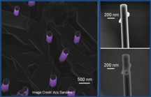 |
| The helium ion microscope has high depth of focus and resolution providing researchers with images of gallium nitride nanowires that would be impossible to produce with electron microscopy. In addition, helium ions provide the ability to etch very precisely. |
Abstract:
NIST is taking a huge step into the ultra-small with the Precision Imaging Facility (PIF) now being outfitted in new Precision Measurement Laboratory on the Boulder campus. The PIF, which houses some of the most advanced imaging instruments in the world, will give researchers the ability to dissect, create, and catalog technologically important materials and devices at the atomic level, and will fill researchers' microscopy and microanalysis needs for years to come. Completion is scheduled for mid-2012.
Looking At and Into the Ultra-Small
Boulder, CO | Posted on June 13th, 2012A suite of four new instruments and supporting equipment "will directly benefit a broad spectrum of NIST/Boulder's already successful projects," says PIF's Aric Sanders of PML's Quantum Electronics and Photonics Division. "In particular, they will impact projects that create advanced quantum sensors, conduct nanowire-based renewable energy metrology, devise chip-scale atomic clocks and nanoscale magnetic devices, and investigate the reliability of nanomaterials."
The specifications for the 3000-square-foot, shared-use facility were determined by a collaboration of groups at NIST/Boulder, including PML's Time and Frequency, Quantum Electronics and Photonics, and Electromagnetics divisions, as well as the Thermophysical Properties and Materials Reliability divisions of NIST's Material Measurement Laboratory.
The PIF's technological capabilities - the most sophisticated available outside certain Department of Energy facilities - will particularly benefit programs which rely on the complicated interworking of nanoscale materials and microfabrication technology that can only be probed by advanced imaging tools. Eventually, the full suite of instruments will include an aberration-corrected transmission electron microscope (TEM), a combination focused ion beam/scanning electron beam microscope (FIB/SEM), a helium ion microscope, and a local electrode atom probe (LEAP).
Image of gallium nitride nanowires.
The helium ion microscope has high depth of focus and resolution providing researchers with images of gallium nitride nanowires that would be impossible to produce with electron microscopy. In addition, helium ions provide the ability to etch very precisely. (Click image to enlarge.)
Each instrument offers distinctive advantages for measurement and analysis.
The TEM opens the door to sub-angstrom (1 � = 10-10 m) resolution imaging necessary for the characterization of crystalline materials used for single photon emitters, nanoscale light sources, and advanced quantum information circuits. The aberration-corrected TEM, the electrons from which pass completely through the specimen and are imaged on the other side, can locally investigate chemical composition, creating the ability to evaluate directly the results of advanced crystal growth techniques needed for the next generation of such devices.
The FIB/SEM combines two functions that together enable highly precise, three-dimensional manipulation and preparation of samples. A focused beam of ions selectively mills devices and materials at nanometer scales, while the sample is also imaged by an SEM. The combination can reveal internal structure in exquisite detail, and provides an indispensable tool for the preparation of samples for the other analytical techniques such as atom probe and transmission electron microscopy.
The helium ion microscope provides a completely new methodology for imaging surfaces of biological and inorganic materials. Because of the nature of helium ion-sample interactions , this tool also provides the ability to pattern samples without the limitations of imposed by electron beam techniques thus opening the path to devices of sub-10 nm sizes with sub-15 nm spacing.
Local-Electrode Atom Probe (LEAP) devices produce the highest spatial resolution currently available for analyzing specimens at the nanoscale. The PIF's LEAP, when installed, will reconstruct analytic volumes atom by atom, revealing the location and chemical composition of structures invisible to other methods. In particular it has a sensitivity to atomic species and location that is unmatched in other analytic instruments. The atom probe is the only microscope that can achieve 1 part per million resolution in chemistry and effectively single atomic spatial resolution. Although averaging techniques can yield higher chemical resolution (1 He atom in 106 Si atoms, for example) they average over a larger area to achieve this. The new LEAPwill offer NIST researchers the ability to investigate, for example, the distribution of dopants in nanoscale semiconductor devices.
The capabilities of these four instruments, coupled with the associated sample preparation and inspection resources also housed in the PIF, provide uniquely powerful abilities to NIST and potentially, through focused collaborations, to the broader scientific community.
Operation of the PIF is modeled on the very successful cooperative Boulder microfabrication facility which has been in existence for many years. In this operational model all projects at NIST Boulder have access to the PIF and the extension and refinement of the facility and its resources evolves continually to meet the needs of NIST's world-class research.
####
About National Institute of Standards and Technology (NIST)
The National Institute of Standards and Technology (NIST) is an agency of the U.S. Department of Commerce.
Any mention or image of commercial products within NIST web pages is for information only; it does not imply recommendation or endorsement by NIST.
For more information, please click here
Contacts:
Aric Sanders
303-497-4731
Copyright © National Institute of Standards and Technology (NIST)
If you have a comment, please Contact us.Issuers of news releases, not 7th Wave, Inc. or Nanotechnology Now, are solely responsible for the accuracy of the content.
Bookmark:


| Related News Press |
News and information
![]() Quantum computer improves AI predictions April 17th, 2026
Quantum computer improves AI predictions April 17th, 2026
![]() Flexible sensor gains sensitivity under pressure April 17th, 2026
Flexible sensor gains sensitivity under pressure April 17th, 2026
![]() A reusable chip for particulate matter sensing April 17th, 2026
A reusable chip for particulate matter sensing April 17th, 2026
![]() Detecting vibrational quantum beating in the predissociation dynamics of SF6 using time-resolved photoelectron spectroscopy April 17th, 2026
Detecting vibrational quantum beating in the predissociation dynamics of SF6 using time-resolved photoelectron spectroscopy April 17th, 2026
Imaging
![]() Simple algorithm paired with standard imaging tool could predict failure in lithium metal batteries August 8th, 2025
Simple algorithm paired with standard imaging tool could predict failure in lithium metal batteries August 8th, 2025
![]() First real-time observation of two-dimensional melting process: Researchers at Mainz University unveil new insights into magnetic vortex structures August 8th, 2025
First real-time observation of two-dimensional melting process: Researchers at Mainz University unveil new insights into magnetic vortex structures August 8th, 2025
![]() New imaging approach transforms study of bacterial biofilms August 8th, 2025
New imaging approach transforms study of bacterial biofilms August 8th, 2025
Laboratories
![]() Researchers develop molecular qubits that communicate at telecom frequencies October 3rd, 2025
Researchers develop molecular qubits that communicate at telecom frequencies October 3rd, 2025
Govt.-Legislation/Regulation/Funding/Policy
![]() Quantum computer improves AI predictions April 17th, 2026
Quantum computer improves AI predictions April 17th, 2026
![]() Metasurfaces smooth light to boost magnetic sensing precision January 30th, 2026
Metasurfaces smooth light to boost magnetic sensing precision January 30th, 2026
![]() New imaging approach transforms study of bacterial biofilms August 8th, 2025
New imaging approach transforms study of bacterial biofilms August 8th, 2025
Announcements
![]() A fundamentally new therapeutic approach to cystic fibrosis: Nanobody repairs cellular defect April 17th, 2026
A fundamentally new therapeutic approach to cystic fibrosis: Nanobody repairs cellular defect April 17th, 2026
![]() UC Irvine physicists discover method to reverse �quantum scrambling� : The work addresses the problem of information loss in quantum computing system April 17th, 2026
UC Irvine physicists discover method to reverse �quantum scrambling� : The work addresses the problem of information loss in quantum computing system April 17th, 2026
Tools
![]() Metasurfaces smooth light to boost magnetic sensing precision January 30th, 2026
Metasurfaces smooth light to boost magnetic sensing precision January 30th, 2026
![]() From sensors to smart systems: the rise of AI-driven photonic noses January 30th, 2026
From sensors to smart systems: the rise of AI-driven photonic noses January 30th, 2026
![]() Japan launches fully domestically produced quantum computer: Expo visitors to experience quantum computing firsthand August 8th, 2025
Japan launches fully domestically produced quantum computer: Expo visitors to experience quantum computing firsthand August 8th, 2025
|
|
||
|
|
||
| The latest news from around the world, FREE | ||
|
|
||
|
|
||
| Premium Products | ||
|
|
||
|
Only the news you want to read!
Learn More |
||
|
|
||
|
Full-service, expert consulting
Learn More |
||
|
|
||