Home > Press > High-resolution atomic imaging of specimens in liquid by TEM using graphene liquid cell: Looking into specimens on an atomic level in liquids, and understanding atomic processes so far regarded impossible
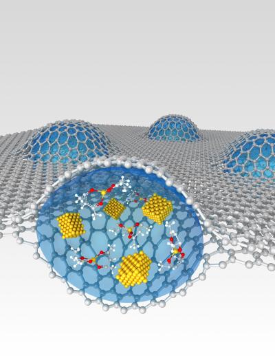 |
| Two sheets of graphene encapsulate a platinum growth solution.
Credit: KAIST |
Abstract:
Daejeon, the Republic of Korea, April 9, 2012—The Korea Advanced Institute of Science and Technology (KAIST) announced that a research team from the Department of Materials Science and Engineering has developed a technology that enables scientists and engineers to observe processes occurring in liquid media on the smallest possible scale which is less than a nanometer.
High-resolution atomic imaging of specimens in liquid by TEM using graphene liquid cell: Looking into specimens on an atomic level in liquids, and understanding atomic processes so far regarded impossible
Daejeon, South Korea | Posted on April 9th, 2012Professor Jeong Yong Lee and Researcher Jong Min Yuk, in collaboration with Professor Paul Alivisatos's and Professor Alex Zettl's groups at the University of California, Berkeley, succeeded in making a graphene liquid cell or capsule, confining an ultra-thin liquid film between layers of graphene, for real-time and in situ imagining of nanoscale processes in fluids with atomic-level resolution by a transmission electron microscope (TEM). Their research was published in the April 6, 2012 issue of Science. (http://www.sciencemag.org/content/336/6077/61.abstract)
The graphene liquid cell (GLC) is composed of two sheets of graphene sandwiched to create a sealed chamber where a platinum growth solution is encapsulated in the form of a thin slice. Each graphene layer has a thickness of one carbon atom, the thinnest membrane that has ever been used to fabricate a liquid cell required for TEM.
The research team peered inside the GLC to observe the growth and dynamics of platinum nanocrystals in solution as they coalesced into a larger size, during which the graphene membrane with the encapsulated liquid remained intact. The researchers from KAIST and the UC Berkeley identified important features in the ongoing process of the nanocrystals' coalescence and their expansion through coalescence to form certain shapes by imaging the phenomena with atomic-level resolution.
Professor Lee said,
"It has now become possible for scientists to observe what is happening in liquids on an atomic level under transmission electron microscopes."
Researcher Yuk, one of the first authors of the paper, explained his research work.
"This research will promote other fields of study related to materials in a fluid stage including physical, chemical, and biological phenomena at the atomic level and promises numerous applications in the future. Pending further studies on liquid microscopy, the full application of a graphene-liquid-cell (GLC) TEM to biological samples is yet to be confirmed. Nonetheless, the GLC is the most effective technique developed today to sustain the natural state of fluid samples or species suspended in the liquid for a TEM imaging."
The transmission electron microscope (TEM), first introduced in the 1930s, produces images at a significantly higher resolution than light microscopes, allowing users to examine the smallest level of physical, chemical, and biological phenomena. Observations by TEM with atomic resolution, however, have been limited to solid and/or frozen samples, and thus it has previously been impossible to study the real time fluid dynamics of liquid phases.
TEM imaging is performed in a high vacuum chamber in which a thin slice of the imaged sample is situated, and an electron beam passes through the slice to create an image. In this process, a liquid medium, unlike solid or frozen samples, evaporates, making it difficult to observe under TEM.
Attempts to produce a liquid capsule have thus far been made with electron-transparent membranes of such materials as silicon nitride or silicon oxide; such liquid capsules are relatively thick (tens to one hundred nanometers), however, resulting in poor electron transmittance with a reduced resolution of only a few nanometers. Silicon nitride is 25 nanometers thick, whereas graphene is only 0.34 nanometers.
Graphene, most commonly found in bulk graphite, is the thinnest material made out of carbon atoms. It has unique properties such as mechanical tensile strength, high flexibility, impermeability to small molecules, and high electrical conductivity. Graphene is an excellent material to hold micro- and nanoscopic objects for observation in a transmission electron microscope by minimizing scattering of the electron beam that irradiates a liquid sample while reducing charging and heating effects.
####
For more information, please click here
Contacts:
Lan Yoon
82-423-502-295
Copyright © The Korea Advanced Institute of Science and Technology (KAIS
If you have a comment, please Contact us.Issuers of news releases, not 7th Wave, Inc. or Nanotechnology Now, are solely responsible for the accuracy of the content.
Bookmark:


| Related News Press |
News and information
![]() Quantum computer improves AI predictions April 17th, 2026
Quantum computer improves AI predictions April 17th, 2026
![]() Flexible sensor gains sensitivity under pressure April 17th, 2026
Flexible sensor gains sensitivity under pressure April 17th, 2026
![]() A reusable chip for particulate matter sensing April 17th, 2026
A reusable chip for particulate matter sensing April 17th, 2026
![]() Detecting vibrational quantum beating in the predissociation dynamics of SF6 using time-resolved photoelectron spectroscopy April 17th, 2026
Detecting vibrational quantum beating in the predissociation dynamics of SF6 using time-resolved photoelectron spectroscopy April 17th, 2026
Imaging
![]() Simple algorithm paired with standard imaging tool could predict failure in lithium metal batteries August 8th, 2025
Simple algorithm paired with standard imaging tool could predict failure in lithium metal batteries August 8th, 2025
Graphene/ Graphite
![]() Electrifying results shed light on graphene foam as a potential material for lab grown cartilage June 6th, 2025
Electrifying results shed light on graphene foam as a potential material for lab grown cartilage June 6th, 2025
![]() Breakthrough in proton barrier films using pore-free graphene oxide: Kumamoto University researchers achieve new milestone in advanced coating technologies September 13th, 2024
Breakthrough in proton barrier films using pore-free graphene oxide: Kumamoto University researchers achieve new milestone in advanced coating technologies September 13th, 2024
Discoveries
![]() Quantum computer improves AI predictions April 17th, 2026
Quantum computer improves AI predictions April 17th, 2026
![]() Flexible sensor gains sensitivity under pressure April 17th, 2026
Flexible sensor gains sensitivity under pressure April 17th, 2026
![]() A reusable chip for particulate matter sensing April 17th, 2026
A reusable chip for particulate matter sensing April 17th, 2026
![]() Detecting vibrational quantum beating in the predissociation dynamics of SF6 using time-resolved photoelectron spectroscopy April 17th, 2026
Detecting vibrational quantum beating in the predissociation dynamics of SF6 using time-resolved photoelectron spectroscopy April 17th, 2026
Announcements
![]() A fundamentally new therapeutic approach to cystic fibrosis: Nanobody repairs cellular defect April 17th, 2026
A fundamentally new therapeutic approach to cystic fibrosis: Nanobody repairs cellular defect April 17th, 2026
![]() UC Irvine physicists discover method to reverse ‘quantum scrambling’ : The work addresses the problem of information loss in quantum computing system April 17th, 2026
UC Irvine physicists discover method to reverse ‘quantum scrambling’ : The work addresses the problem of information loss in quantum computing system April 17th, 2026
Tools
![]() Metasurfaces smooth light to boost magnetic sensing precision January 30th, 2026
Metasurfaces smooth light to boost magnetic sensing precision January 30th, 2026
![]() From sensors to smart systems: the rise of AI-driven photonic noses January 30th, 2026
From sensors to smart systems: the rise of AI-driven photonic noses January 30th, 2026
![]() Japan launches fully domestically produced quantum computer: Expo visitors to experience quantum computing firsthand August 8th, 2025
Japan launches fully domestically produced quantum computer: Expo visitors to experience quantum computing firsthand August 8th, 2025
|
|
||
|
|
||
| The latest news from around the world, FREE | ||
|
|
||
|
|
||
| Premium Products | ||
|
|
||
|
Only the news you want to read!
Learn More |
||
|
|
||
|
Full-service, expert consulting
Learn More |
||
|
|
||