Home > Press > Hitachi Launches World’s Highest Resolution FE-SEM
 |
Abstract:
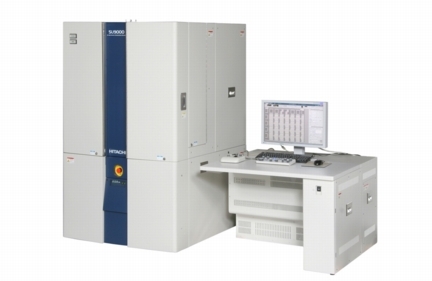
The new SU9000 Field Emission (FE) Scanning Electron Microscope (SEM) from Hitachi High-Technologies features novel electron optics which allow 0.4 nm resolution to be achieved at an accelerating voltage of 30 kV, with a usable magnification up to 3 Million times. This is believed to be the highest resolution-performance currently achievable on a commercially available instrument.
Hitachi Launches World’s Highest Resolution FE-SEM
Maidenhead, UK | Posted on May 31st, 2011Featuring a new type of cold FE electron source with excellent stability and brightness and utilising Hitachi's 25 year experience of in-lens detection technology, the SU9000 also provides outstanding ultra-low current and low voltage imaging of sensitive materials. This excellent all-round performance, combined with fast specimen exchange times and the optional scanning transmission (STEM) modes, makes the SU9000 the ideal choice for use in applications ranging from semiconductor devices, electronics, and advanced nanotechnology materials, to life sciences and medicine.
The new, cold FE electron source delivers probe current that is approximately double that of earlier models, giving high quality images with superior S/N and exceptional stability from the moment the electron beam is switched on. The high performance electron optics allow a resolution of 1.2 nm at an accelerating voltage of 1 kV to be achieved without the need for beam deceleration technology. This greatly simplifies low energy imaging and significantly increases sample throughput.
Hitachi's unique dual through-the-lens detection system allows filtering of electrons of different energies, to give the capability for simultaneous multi-signal imaging. This provides extraordinary versatility for the imaging of structures and surface properties.
Using the scanning transmission (STEM) option, the SU9000 guarantees STEM resolution that can allow the lattice structure of graphite (C (002) d=0.34 nm) to be imaged at 30 kV accelerating voltage. The unique STEM detection system allows simultaneous bright field and dark field imaging and annular DF detection with selectable scattering angle. Up to 4 signals can be simultaneously displayed.
The SU9000 features side-entry sample insertion and can be ready for high resolution imaging in as little as 6 minutes or less; the fast exchange times benefiting from the high stability of the electron beam.
An order of magnitude better vacuum around the sample minimizes contamination, enhancing resolution and eliminating the need for an additional cold trap for cryo work on biological samples.
Ease of use is guaranteed through a new user interface, while a large 24.1-inch widescreen monitor offers a comfortable environment for both operating the instrument and viewing images.
####
For more information, please click here
Contacts:
Press Enquiries:
In Press Public Relations Ltd
PO Box 24
Royston, Herts, SG8 6TT
Tel: +44 (0)1763 262621
Internet: www.inpress.co.uk
Other Enquiries:
Hitachi High-Technologies Corporation
Whitebrook Park, Lower Cookham Road
Maidenhead, Berkshire SL6 8YA
Tel: + 44 (0) 800 316 1500
Copyright © Hitachi High-Technologies Corporation
If you have a comment, please Contact us.Issuers of news releases, not 7th Wave, Inc. or Nanotechnology Now, are solely responsible for the accuracy of the content.
Bookmark:


| Related News Press |
News and information
![]() Researchers develop molecular qubits that communicate at telecom frequencies October 3rd, 2025
Researchers develop molecular qubits that communicate at telecom frequencies October 3rd, 2025
![]() Next-generation quantum communication October 3rd, 2025
Next-generation quantum communication October 3rd, 2025
![]() "Nanoreactor" cage uses visible light for catalytic and ultra-selective cross-cycloadditions October 3rd, 2025
"Nanoreactor" cage uses visible light for catalytic and ultra-selective cross-cycloadditions October 3rd, 2025
Imaging
![]() ICFO researchers overcome long-standing bottleneck in single photon detection with twisted 2D materials August 8th, 2025
ICFO researchers overcome long-standing bottleneck in single photon detection with twisted 2D materials August 8th, 2025
![]() Simple algorithm paired with standard imaging tool could predict failure in lithium metal batteries August 8th, 2025
Simple algorithm paired with standard imaging tool could predict failure in lithium metal batteries August 8th, 2025
![]() First real-time observation of two-dimensional melting process: Researchers at Mainz University unveil new insights into magnetic vortex structures August 8th, 2025
First real-time observation of two-dimensional melting process: Researchers at Mainz University unveil new insights into magnetic vortex structures August 8th, 2025
![]() New imaging approach transforms study of bacterial biofilms August 8th, 2025
New imaging approach transforms study of bacterial biofilms August 8th, 2025
Announcements
![]() Rice membrane extracts lithium from brines with greater speed, less waste October 3rd, 2025
Rice membrane extracts lithium from brines with greater speed, less waste October 3rd, 2025
![]() Researchers develop molecular qubits that communicate at telecom frequencies October 3rd, 2025
Researchers develop molecular qubits that communicate at telecom frequencies October 3rd, 2025
![]() Next-generation quantum communication October 3rd, 2025
Next-generation quantum communication October 3rd, 2025
![]() "Nanoreactor" cage uses visible light for catalytic and ultra-selective cross-cycloadditions October 3rd, 2025
"Nanoreactor" cage uses visible light for catalytic and ultra-selective cross-cycloadditions October 3rd, 2025
Tools
![]() Japan launches fully domestically produced quantum computer: Expo visitors to experience quantum computing firsthand August 8th, 2025
Japan launches fully domestically produced quantum computer: Expo visitors to experience quantum computing firsthand August 8th, 2025
![]() Rice researchers harness gravity to create low-cost device for rapid cell analysis February 28th, 2025
Rice researchers harness gravity to create low-cost device for rapid cell analysis February 28th, 2025
|
|
||
|
|
||
| The latest news from around the world, FREE | ||
|
|
||
|
|
||
| Premium Products | ||
|
|
||
|
Only the news you want to read!
Learn More |
||
|
|
||
|
Full-service, expert consulting
Learn More |
||
|
|
||