Home > Introduction > Nanotechnology Glossary N
NANOTECHNOLOGY GLOSSARY N
Last Updated: Tuesday, 04-Jul-2017 06:52:45 PDTThis Nanotechnology Glossary is a work-in-progress, and will be updated very frequently, so check back. Please email us with any missing terms, and we will include them. Any definition that can be attributed to an author will be, unless we get a quote sent to us without one. If you see one for which the author is not shown, and you know who it is, please let us know and we will make the update. Thanks! [brackets] indicate author and copyright holder
- Key to Abbreviations for Original Authors
- Other Future Sciences Glossary Sites
- Robert A. Freitas Jr. Nanomedicine Terms
- A variety of Goo
Nanite: Machines with atomic-scale components. (Popularized by the Star Trek episode "Evolution") As to their weight, a popular question: "Do you 'feel' heavier after you drink a mouthful of water? A mouthful of water, roughly 5 cm^3, would have the same mass as a ~2 terabot (2 trillion nanites) dose of 1 micron^3 nanorobots. You'll never feel it." Robert A. Freitas Jr. "Nanobot" and "Nanorobot" usually mean the same thing.
Nanoarray: an ultra-sensitve, ultra-miniaturized array for biomolecular analysis. BioForce Nanosciences' Nanoarrays utilize approximately 1/10,000th of the surface area occupied by a conventional microarray, and over 1,500 nanoarray spots can be placed in the area occupied by a single microarray domain. [BioForce Nanosciences] See The NanoPro™ System
Nanoassembler: the Holy Grail of nanotechnology; once a perfected nanoassembler is availble, building anything becomes possible, with physics and the imagination the only limitation (of course each item would have to be designed first, which is another small hurdle). See Bootstrapping a Nanofactory "So how hard is it to build a nanofactory? You need to start with a working fabricator, a nanoscale device that can combine individual molecules into useful shapes. But once you have that, the rest is pretty straightforward." —CRN
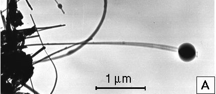
Nanobalance: Simply put, a nanoscale balance for determining mass, small enough to weigh viruses and other sub-micron scale particles. "A mass attached at the end of a nanotube shifts its resonance frequency. If the nanotube is calibrated (i.e., its spring constant known), it is possible to measure the mass of the attached particle." A nanobalance "could be useful for determining the mass of other objects on the femtogram to picogram size range." See Weighing The Very Small.
Transmission electron microscope image shows "nanobalance:" a resonating carbon nanotube used to determine the mass of the attached carbon particle.
Nanarchist: Someone who circumvents government control to use nanotechnology, or someone who advocates this. [Eli Brandt, October 1991]
Nanarchy: The use of automatic law-enforcement by nanomachines or robots, without any human control - see blue goo [Mark S. Miller].
Click for larger version
Thanks to John Toon, Georgia Institute of Technology. © Science Magazine
Nanobarcode: SurroMed's Nanobarcode™ technology uses cylindrically-shaped colloidal metal nanoparticles, in which the metal composition can be alternated along the length and the size of each metal segment can be controlled. Intrinsic differences in reflectivity between the metal segments allow individual particles to be identified by conventional optical microscopy. See SurroMed and Penn State Publish Pioneering Work in the Journal Science Describing Nanobarcode™ Particles
Nanobeads: Polymer beads with diameters of between 0.1 to 10 micrometers. Also called nanodots, nanocrystals and quantum beads. Impregnating fluorescent crystal chips into these beads allows simultaneous measurement of thousands of biological interactions, a stepping stone for breakthroughs in the diagnosis and treatment of disease. ... with the potential to accelerate drug discovery and clinical diagnostics." See Nanodots and Local Mechanical Properties of Cells.
Nanobialys -- Ultra-miniature bialy-shaped particles developed by Washington University as delivery agents for drugs and imaging agents directly to the sites of tumors and plaques.
Nanobiotechnology: applying the tools and processes of MNT to build devices for studying biosystems, in order to learn from biology how to create better nanoscale devices. Should hasten the creation of useful micro devices that mimic living biological systems.
Nanobot: See NaniteNanobubbles: tiny air bubbles on colloid surfaces. Thought to reduce drag, such as would be of benefit to swimmers wearing a suit coverd in them. See First Images of Nanobubbles
Nanocatalysis See LBL-UCB Scientists Demonstrate Nanocatalysis and Nanocluster arrays refine the catalytic process
Nanochips: we are approaching the limits of standard microchip technology; thus, the "nanochip" -- a next-smaller microchip. [ed] They are also a next-gen device for mass storage, of significantly higher density, with greater speed, and much lower cost. [Tod Maffin (p)] See Getting a Line on Nanochips
Nanochondria: Nanomachines existing inside living cells, participating in their biochemistry (like mitochondria) and/or assembling various structures. See also nanosome. [Ken Clements 1996]
Nanocombinatorics: The new analytical method utilizes a technique invented at Northwestern called polymer pen lithography, where basically a rubber stamp having as many as 11 million sharp pyramids is mounted on a transparent glass backing and precisely controlled by an atomic force microscope to generate desired patterns on a surface. Each pyramid -- a polymeric pen -- is coated with molecules for a particular purpose. Nanocombinatorics holds promise for screening catalysts for energy conversion, understanding properties conferred by nanostructures, identifying active molecules for drug discovery or even optimizing materials for tissue regeneration, among other applications.
Nanocomputer: A computer made from components (mechanical, electronic, or otherwise) built at the nanometer scale. These computers could be many orders-of-magnititude faster than today's, which enables software to take proportional leaps.Nanocones: Nonplanar graphitic structures. Carbon-based structures with five-fold symmetry that form due to disclination defects in two-dimensional graphene sheets. They have been observed as nanotube caps and as freestanding structures. [North Carolina State University] See Nanostructures Fabrication from Carbon Nanocones
Nanocontainers: "Micellar nanocontainers" or "Micelles," these are nanoscale polymeric containers that could be used to selectively deliver hydrophobic drugs to specific sites within individual cells. See Nanocontainers deliver on drugs.
Nanocrystals: also known as nanoscale semiconductor crystals. "Nanocrystals are aggregates of anywhere from a few hundred to tens of thousands of atoms that combine into a crystalline form of matter known as a "cluster." Typically around ten nanometers in diameter, nanocrystals are larger than molecules but smaller than bulk solids and therefore frequently exhibit physical and chemical properties somewhere in between. Given that a nanocrystal is virtually all surface and no interior, its properties can vary considerably as the crystal grows in size." [LBL] See Nanocrystals: The shapes of things to come
The first atomic-scale images of nanocrystals that help reduce pollution show a surprising triangular, rather than hexagonal, shape. The new information should help researchers improve the chemical process.
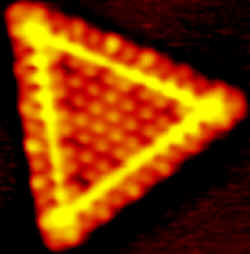 |
Phys. Rev. Lett. 84, 951 (2000). Atomic-Scale Structure of Single-Layer MoS2 Nanoclusters. S. Helveg, J. V. Lauritsen, E. L�gsgaard, I. Stensgaard, J. K. N�rskov, B. S. Clausen, H. Tops�e, and F. Besenbacher
Thanks to Physical Review Letters & Dr. Flemming Besenbacher, University of Aarhus, Denmark © American Physical Society |
| Click for larger version |
"Nanocrystals might be used to make super-strong and long-lasting metal parts. The crystals also might be added to plastics and other metals to make new types of composite structures for everything from cars to electronics." See Discovery could bring widespread uses for 'nanocrystals'. Single atoms caged inside nanocrystals gives you a "quantum confined atom", or QCA, "with potential uses ranging from clear-glass sunglasses to bio-sensors to optical computing and just about anything optical in between." See Researchers Turn Scrap to Strength with Nanocrystals.
Single-electron transistor (SET) is a three terminal device, where single electron current between a source and a drain through a nanocrystal is controlled by a gate. The nanocrystals are the tiny light specs.
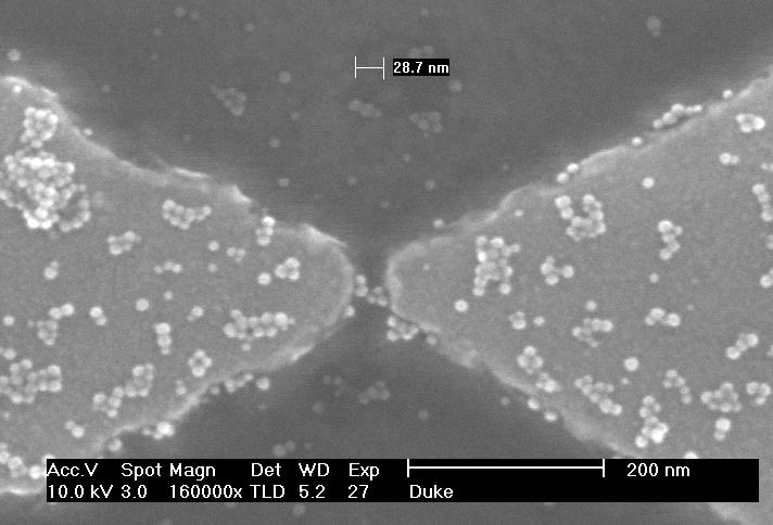 |
Thanks to Professor Gleb Finkelstein, Physics Department. © Duke University |
| Click for larger version |
Nano Cubic Technology: an ultra-thin layer coating that results in higher resolution for recording digital data, ultra-low noise and high signal-to-noise ratios that are ideal for magneto-resistive (MR) heads. It is capable of catapulting data cartridge and digital videotape to one-terabyte native (uncompressed) capacities and floppy disk capacities to three gigabytes. To help visualize the potential, 1TB can store up to 200 two-hour movies. [Fuji Photo Film U.S.A., Inc.]
Nanodefenses: any of the "good" goo's, such a Blue Goo. Protectors against Grey Goo, destructive nanoswarms, and the like.Nanodisaster: See the various 'goo' scenerios that have potentially negative outcomes.
NEMS - nanoelectromechanical systems: A generic term to describe nano scale electrical/mechanical devices. [ZY]
Nanoelectronics: Electronics on a nanometer scale, whether made by current techniques or nanotechnology; includes both molecular electronics and nanoscale devices resembling today's semiconductor devices. [NTN]
Nanofabrication: construction of items using assemblers and stock molecules. See Nanofacture. AKA: nanoscale engineering.Nanofacture: The fabrication of goods using nanotechnology [Geoff Dale 1995]. See Nanofabrication
Nanofilters: One opportunity for nanoscale filters is for the separation of molecules, such as proteins or DNA, for research in genomics. See Selective nanofilters for proteins, DNA Another, as "masks to prevent exposure to biological pathogens such as viruses that can be as small as 30 nanometers in diameter." See Biologically inspired nanotechnology. Another use is in water filtration.
Nanofluidics: controlling nano-scale amounts of fluids
Nanogate: A device that precisely meters the flow of tiny amounts of fluid. Precise control of the flow restriction is accomplished by deflecting a highly polished cantilevered plate. The opening is adjustable on a sub-nanometer scale, limited by the roughness of the polished plates. Thus, the Nanogate is an Ultra Surface Finish Effect Mechanism (USFEM). The Nanogate can be fabricated on a macro-, meso- or micro- (MEMs) scale. [James R. White]
See Nanogate: A Fundamental New Device for Nanofluidics
|
Nanoguitar: "Made for fun to illustrate the technology -- the world's smallest guitar is 10 micrometers long -- about the size of a single cell -- with six strings each about 50 nanometers, or 100 atoms, wide. Just one of several structures that Cornell researchers believe are the world's smallest silicon mechanical devices. Researchers made these devices at the Cornell Nanofabrication Facility, bringing microelectromechanical devices, or MEMS, to a new, even smaller scale -- the nano-sized world." See World's smallest silicon mechanical devices are made at Cornell. |
Smallest guitar, about the size of a human blood cell, carved out of crystalline silicon, illustrates new technology for nanosized electromechanical devices. 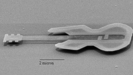
Click for larger version Thanks to Professor Harold Craighead and Dustin Carr. © Cornell University |
Nanogypsy: someone who travels form place to place, spreading the "nano" word. Usually a person who takes the most optimistic viewpoint, and is enthusitic. [uhf]
Nanohorns: One of the SWNT (single walled carbon nanotube) types, with an irregular horn-like shape, which may be a critical component of a new generation of fuel cells. "The main characteristic of the carbon nanohorns is that when many of the nanohorns group together an aggregate (a secondary particle) of about 100 nanometers is created. The advantage being, that when used as an electrode for a fuel cell, not only is the surface area extremely large, but also, it is easy for the gas and liquid to permeate to the inside. In addition, compared with normal nanotubes, because the nanohorns are easily prepared with high purity it is expected to become a low-cost raw material." See NEC uses Carbon Nanotubes to Develop a Tiny Fuel Cell for Mobile Applications and here is a TEM image.
Nanoimprinting: Sometimes called soft lithography. A technique that is very simple in concept, and totally analogous to traditional mould- or form-based printing technology, but that uses moulds (masters) with nanoscale features. As with the printing press, the potential for mass production is clear. There are two forms of nanoimprinting, one that uses pressure to make indentations in the form of the mould on a surface, the other, more akin to the printing press, that relies on the application of "ink" applied to the mould to stamp a pattern on a surface. Other techniques such as etching may then follow. [CMP]
Nanoimprint Machine: a form of soft lithographyNanohacking: describes what MNT is all about -- "hacking" at the molecular level.
Nanoindentation: Nanoindentation is similar to conventional hardness testing performed on a much smaller scale. The force required to press a sharp diamond indenter into a material is measured as a function of indentation depth. As depth resolution is on the scale of nanometers (hence the name of the instrument), it is possible to conduct indentation experiments even on thin films. Two quantities which can be readily extracted from nanoindentation experiments are the material's modulus, or stiffness, and its hardness, which can be correlated to yield strength. Investegators have also used nanoindentation to study creep, plastic flow, and fracture of materials. [Nix Research Group, Materials Science & Engineering, Stanford University]
Nanolithography: Writing on the nanoscale. From the Greek words Nanos - Dwarf, Lithos - rock, and grapho - to write, this word literally means "small writing on rocks." [NTN] See definition in Wikipedia.
Nanomachine: An artificial molecular machine of the sort made by molecular manufacturing. [FS]Nanomachining: like traditional machining, where portions of the structure are removed or modified, nanomachining involves changing the structure of nano-scale materials or molecules.
nanoManipulator: uses virtual reality (VR) goggles and a force feedback probe as an interface to a scanning probe microscope, providing researchers with a new way to interact with the atomic world. Researchers can travel over genes, tickle viruses, push bacteria around, and tap on molecules - the nanoManipulator simplifies the process and allows researchers to play with their atoms. University of North Carolina at Chapel Hill (UNC-CH) The Nanomanipulator from the Center for Computer Integrated Systems for Microscopy and Manipulation (CISMM) at UNC Chapel Hill. Part of the Nanoscale Science Research Group (NSRG). Images & Movies with Microscopes
Nanomanipulation: The process of manipulating items at an atomic or molecular scale in order to produce precise structures. [ZY See Zyvex SEM manipulator]
Nanomanufacturing: Same as molecular manufacturing.Nanomaterials: can be subdivided into nanoparticles, nanofilms and nanocomposites. The focus of nanomaterials is a bottom up approach to structures and functional effects whereby the building blocks of materials are designed and assembled in controlled ways. [Oxonica]
Nanomedicine: See Nanomedicine Glossary|
Vapour grown carbon fibres are obtained as shown in this SEM image. The diameters of these fibres can vary from 100 nm to 500 nm.
|
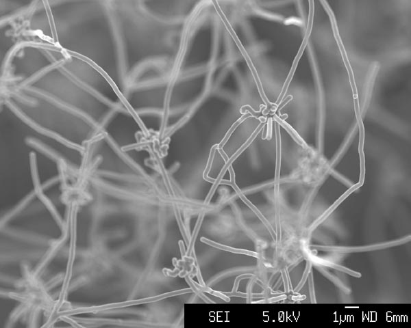
Nanomesh and Nanofibres: (or "Nanofibers") This term covers CNT's (see above), and as described here, the other "nanoscale fibers" referred to as "polymeric" (made from polymers). Currently used in air and liquid filtration applications. Using a process called "electrospinning" - or e-spin - a polymer "mesh" is formed into a nanofiber membrane, hense "nanomesh", with 150 - 200 nm diameters. Some have been made since 1970, but were not called "nano" until recently. One potential use is "to prevent body tissues from sticking together as they heal. It also breaks down in the body over time like biodegradable sutures." , which makes it a surgical material for the 21st Century. Other uses include biomedical devices, filtration systems, and dust collecting systems. See Biodegradable nanofiber could prevent scar tissue. |
"Ultra-Web(R) nanofiber" produced on a Scanning Electron Microscope (SEM).
|
Nano-Optics: Interaction of light and matter on the nanoscale. See University of Rochester - Institute of Optics - NANO-OPTICS GROUP
Nanopens & Nanopencils: (AKA: Atomic Pencil) "Analogous to using a quill pen but on a billionth the scale", and may transform dip-pen nanolithography. Allows for drawing electronic circuits a thousand times smaller than current ones. The "pen" is an atomic force microscope (AFM). See Nanopipettes and Nanoplotter for further details.
NanoPGM - nanometer-scale patterned granular motion: The goal of NanoPGM is to generate millions of �nanofingers,� finger-like structures each only a few nanometers long, that might someday perform precise, massively parallel manipulation of molecules and directed assembly of other nanometer-scale objects. This ability answers one of the biggest technical challenges facing builders of nanocomputers: how to arrange as many as a trillion molecular computing components in an area only a few millimeters square. [MITRE / Alex Wissner-Gross]
Nanopharmaceuticals: nanoscale particles used to modulate drug transport for drug uptake and delivery applications.
Nanophase Carbon Materials (carbon nanotubes, nanodiamond, nanocomposite]--A form of matter in which small clusters of atoms form the building blocks of a larger structure. These structures differ from those of naturally occurring crystals, in which individual atoms arrange themselves into a lattice.
Nanopipettes: "Cantilevered/Straight Nanopipettes can be used as nanopens for controlled chemical delivery or removal from regions as small as 100 nanometers. They can also be used as vessels for containing molecules whose optical properties change in response to their chemical environment." Other uses include "controlled chemical etching with the precision of atomic force microscopy; chemical imaging of surfaces; delivering femtosecond laser pulses; and performing NSOM/SNOM imaging using a UV excimer laser." See Cantilevered/Straight Nanopipettes Modifying the nanopipette yields other nanotools, such as Nanotweezers and Nanoheaters. See Nanotools.
Nanoplotter: A multi-tip nanopen. "A device that can draw patterns of tiny lines just 30 molecules thick and a single molecule high. ... produces eight identical patterns at once and extends ... dip-pen nanolithography towards mass producing nanoscale devices and circuits by converting what was a serial process to a parallel one. May be use to "... miniaturize electronic circuits, pattern precise arrays of organic and biomolecules such as DNA and put thousands of different medical sensors on an area much tinier than the head of a pin." See Plotting Chemicals and Nanoplotter with Parallel Writing Capabilities (PDF).
Nanopores: Involves squeezing a DNA sequence between two oppositely charged fluid reservoirs, separated by an extremely small channel. Essentially itty bitty tiny holes. Nanoscopic pores found in purpose-built filters, sensors, or diffraction gratings to make them function better. See Influencing structure in the heart of nanoland. As activated carbon, they may also be used as an alternative fuel storage medium, due to their massive internal surface area. "Scientists believe nanopores, tiny holes that allow DNA to pass through one strand at a time, will make DNA sequencing more efficient." See Understanding Nanodevices -- Nanopores. In biology, they are "complex protein assemblies that span cell membranes and allow ionic transport across the otherwise impermeable lipid bilayer. Nanopores are important because while some pores help maintain cell homeostasis, others disrupt cell function." See Towards Fabrication of Solid-State Mimics of Biological Nanopores. "A nanopore can be a protein channel in a lipid bilayer or an extremely small isolated 'hole' in a thin, solid-state membrane" such that "DNA and RNA, can be registered and characterized singly ..." See Developing Nanopores as Probes and The Nanopore Project.
Nanoprobe: Nanoscale machines used to diagnose, image, report on, and treat disease within the body. See "Cell Repair Machine", "Nanites", "Nanobots", and "Nanomachine". Also: tips for scanning probe microscopes.
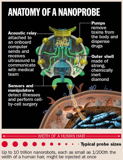
Courtesy of, and Copyright 1999 by Time Inc. Reprinted by Permission.
"Anatomy of a Nanoprobe" by Joe Lertola. 11/08/99 issue of Time.
Reproduction strictly prohibited without permission of Time.
Click for larger image
Nanorods: or Carbon Nanorods. Formed from multi-wall carbon nanotubes. Another nanoscale material with unique and promising physical properties, such that may yield improvements in high-density data storage, and allow for cheaper flexible solar cells. See Three Element Nanorods and Flexible and Inexpensive Solar Cells Based on Inorganic Nanorods..
Nanoropes: nanotubes connected and strung together.
Nanoscale: 1 - 100 nanometer range.
Nanoscopic Scale same as nanoscale.
Nanosensors: nanoscale sensors.
Nanoshells: Nanoscale metal spheres, which can absorb or scatter light at virtually any wavelength. "The nanoshells act as an amazingly versatile optical component on the nanometer scale: they may provide a whole new approach to optical materials and components," Professor Naomi Halas. See Nanoshells May Be Key To Next Wave Of Light-Based Technology and Physics of Nanoshells.
Nanosources: sources that emit light from nanometre-scale volumes. [See Tears of brilliance Nature reg. req'd]
Nanosome: Nanodevices existing symbiotically inside biological cells, doing mechanosynthesis and disassembly for it and replicating with the cell. Similar to nanochondria. [AS January 1998]
Nanosprings: A nanowire wrapped into a helix. Speculation is that they "may someday make highly sensitive magnetic field detectors, perhaps finding application in hard drive read heads. Alternatively, nanosprings could serve as positioners, or even as tiny conventional springs, for nanomachines of the future." See Spiraling in on Nanosprings and Nanosprings jump into place.
Nanosurgery: A generic term including molecular repair and cell surgery. [FS] See Voyage of the Nano-SurgeonsNanoswarm: UFog and Goo
Nanotechism: the religion of nanotech, as opposed to the science of nanotech
Nanotechnology: a manufacturing technology able to inexpensively fabricate most structures consistent with natural law, and to do so with molecular precision. [FS]
Nanoterrorism: using MNT derived nanites to do damage to people or places.|
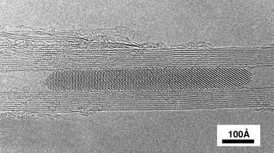
Nano-test-tubes: CNT's opened and filled with materials, and used to carry out chemical reactions. See The Opening and Filling of Multi-Walled Carbon Nanotubes (MWTs) and The Opening and Filling of Single-Walled Carbon Nanotubes (SWTs). |
A High Resolution Transition Electron Micrograph (TEM) of Samarium Oxide Inside a Multi-Walled Carbon Nanotube.
|
Nanotribology: the methodical study of friction, lubrication, and wear at the nanoscale.
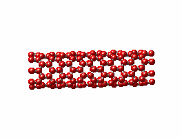
Nanotube: See our Nanotubes and Buckyballs page
Copyright Prof. Vincent H. Crespi Department of Physics Pennsylvania State University.
And an excellent description of Nanotubes
A one dimensional fullerene (a convex cage of atoms with only hexagonal and/or pentagonal faces) with a cylindrical shape. Carbon nanotubes discovered in 1991 by Sumio Iijima resemble rolled up graphite, although they can not really be made that way. Depending on the direction that the tubes appear to have been rolled (quantified by the 'chiral vector'), they are known to act as conductors or semiconductors. Nanotubes are a proving to be useful as molecular components for nanotechnology. [Encyclopedia Nanotech]
Strictly speaking, any tube with nanoscale dimensions, but generally used to refer to carbon nanotubes (a commonly mentioned non-carbon variety is made of boron nitride), which are sheets of graphite rolled up to make a tube. The dimensions are variable (down to 0.4 nm in diameter) and you can also get nanotubes within nanotubes, leading to a distinction between multi-walled and single-walled nanotubes. Apart from remarkable tensile strength, nanotubes exhibit varying electrical properties (depending on the way the graphite structure spirals around the tube, and other factors), and can be insulating, semiconducting or conducting (metallic). [CMP]
AKA: Multiwall Carbon Nanotubes (MWNTs), Single Walled Carbon Nanotubes (SWCNs)
See Nanobeam Mechanics: Elasticity, Strength, and Toughness of Nanorods and Nanotubes and
Fullerene Nanotubes: C1,000,000 and Beyond. Boris I. Yakobson and Richard E. Smalley.
and here Carbon Nanotubes in Space
"Maybe the most significant spin-off product of fullerene research....are nanotubes based on carbon or other elements. These systems consist of graphitic sheets seamlessly wrapped to cylinders. With only a few nanometers in diameter, yet (presently) up to a millimeter long, the length-to-width aspect ratio is extremely high. A truly molecular nature is unprecedented for macroscopic devices of this size. Accordingly, the number of both specialized and large-scale applications is growing constantly."
See [The Nanotube Site]
Nanowires: "Semiconductor nanowires are one-dimensional structures, with unique electrical and optical properties, that are used as building blocks in nanoscale devices." See Nanowires within nanowires and Learning how to Fabricate Nanowire. "Striped or 'superlatticed' nanowires can function as transistors, LEDs (light-emitting diodes) and other optoelectronic devices, biochemical sensors, heat-pumping thermoelectric devices, or all of the above, along the same length of wire." See Nanowires Get Their Stripes.
Nanny: A cell-repair nanite
NEMS - Nanoelectromechanical systems: Nanoscale MEMS.
nm: Abbreviation for Nanometer.
NRAM™ - Nanotube-based/Nonvolatile RAM, developed by Nantero, using proprietary concepts and methods derived from leading-edge research in nanotechnology.
Nanowetting: how wetting behavior depends on nanoscale topography on a substrate. [BNL]
NBIC: Nanotechnology, Biotechnology, Information Technology and Cognitive Science. See Converging Technologies for Improving Human Performance
NE3LS: Nanotechnology's Ethical, Environmental, Economic, Legal, and Social Implications. From 'Mind the gap': science and ethics in nanotechnology. click here (requires free registration) [Anisa Mnyusiwalla, Abdallah S. Daar and Peter A. Singer 2003 Nanotechnology 14 R9-R13. 13 Feb 2003]
Back To Top
Key to Abbreviations for Original Authors
Other Future Sciences, Nanotech and Nanoscience glossary sites
![]() ASTM
ASTM
![]() Foresight
Foresight
![]() IoN
IoN
![]() Zyvex
Zyvex
![]() Nanotechnology Part One: Taxonomy Codesta
Nanotechnology Part One: Taxonomy Codesta
![]() Nanomedicine Book Glossary R A Freitas Jr.
Nanomedicine Book Glossary R A Freitas Jr.
![]() JPK Instruments NanoBiotechnology Glossary (click NanoResources/Glossary)
JPK Instruments NanoBiotechnology Glossary (click NanoResources/Glossary)
![]() Nanoword Steve Lenhert
Nanoword Steve Lenhert
![]() Lextropicon: Extropian Neologisms Max More
Lextropicon: Extropian Neologisms Max More
![]() Transhuman Terminology Anders Sandberg
Transhuman Terminology Anders Sandberg
![]() Accelerating Future Lexicon Michael Anissimov
Accelerating Future Lexicon Michael Anissimov
![]() Terminology From The Omega Point Theory List
Terminology From The Omega Point Theory List
![]() Orion's Arm Glossary M.Alan Kazlev, et al
Orion's Arm Glossary M.Alan Kazlev, et al
![]() Russian Society of Scanning Probe Microscopy and Nanotechnology.
Russian Society of Scanning Probe Microscopy and Nanotechnology.
|
|
||
|
|
||
| The latest news from around the world, FREE | ||
|
|
||
|
|
||
| Premium Products | ||
|
|
||
|
Only the news you want to read!
Learn More |
||
|
|
||
|
Full-service, expert consulting
Learn More |
||
|
|
||