Home > Press > Scientists take control of magnetism at the microscopic level: Neutrons reveal remarkable atomic behavior in thermoelectric materials for more efficient conversion of heat into electricity
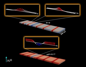 |
| The sample (gray) has no applied magnetic field and has left-handed (left inset) and right-handed (right inset) magnetic domain walls. When magnetized (red), the sample’s domain walls move closer together and either annihilate or combine (bottom inset). CREDIT Image courtesy of Oak Ridge National Laboratory. |
Abstract:
The Science
Atoms in magnetic materials are organized into regions called magnetic domains. Within each domain, the electrons have the same magnetic orientation. This means their spins point in the same direction. “Walls” separate the magnetic domains. One type of wall has spin rotations that are left- or right-handed, known as having chirality. When subjected to a magnetic field, chiral domain walls approach one another, shrinking the magnetic domains. Researchers have developed a magnetic material whose thickness determines whether chiral domain walls have the same or alternating handedness. In the latter case, applying a magnetic field leads to annihilation of colliding domain walls. The researchers combined neutron scattering and electron microscopy to characterize these internal, microscopic features, leading to better understanding of the magnetic behavior.
Scientists take control of magnetism at the microscopic level: Neutrons reveal remarkable atomic behavior in thermoelectric materials for more efficient conversion of heat into electricity
Washington, DC | Posted on August 26th, 2022The Impact
An emerging field of technology called spintronics involves processing and storing information by harnessing an electron’s spin instead of its charge. The ability to control this fundamental property could unlock new possibilities for developing electronic devices. Compared to current technology, these devices could store more information in less space and operate at higher speeds with less energy consumption. This study demonstrates a way to change the rotational direction and occurrence of domain wall pairs. This suggests a potential route for controlling domain walls’ properties and movement. The results could have implications for technologies based on spintronics.
Summary
The ability to manipulate domain wall movement has remained a challenge because typically magnetic domains can randomly switch orientations. In addition, domain boundaries move unpredictably when domain sizes are reduced to accommodate higher information storage density. However, a class of materials called chiral magnets has shown potential for mitigating random domain wall behavior. This is because chiral magnets exhibit intricate spin structures, which help reduce the random reversal of domains.
Researchers from Indiana University–Purdue University Indianapolis, Oak Ridge National Laboratory, Louisiana State University, Norfolk State University, the Peter Grünberg Institute, and the University of Louisiana at Lafayette developed a chiral magnetic material by inserting manganese atoms between hexagonal layers of niobium disulfide compounds. By performing neutron experiments at the High Flux Isotope Reactor (HFIR), the team was able to analyze the magnetic nanostructure of the material when subjected to different temperatures and magnetic fields. These measurements were combined with characterization via Lorentz transmission electron microscopy, allowing a more complete understanding of the magnetic behavior. The team’s data suggest that changing the thickness of the chiral magnet can cause some domain wall pairs to rotate in opposite directions, known as having opposite chirality. Furthermore, the researchers found that domain walls with opposite chirality will move toward each other and annihilate when exposed to an external magnetic field. The findings could inform future research on controlling magnetic properties for technological applications.
Funding
The research was supported by the Department of Energy (DOE) Established Program to Stimulate Competitive Research, the National Science Foundation, the European Research Council, the German Research Foundation, and the Louisiana Board of Regents. Research was performed at High Flux Isotope Reactor at Oak Ridge National Laboratory, a DOE Office of Science user facility.
####
For more information, please click here
Contacts:
Michael Church
DOE/US Department of Energy
Office: 2028416299
Copyright © DOE/US Department of Energy
If you have a comment, please Contact us.Issuers of news releases, not 7th Wave, Inc. or Nanotechnology Now, are solely responsible for the accuracy of the content.
Bookmark:


| Related News Press |
News and information
![]() Quantum computer improves AI predictions April 17th, 2026
Quantum computer improves AI predictions April 17th, 2026
![]() Flexible sensor gains sensitivity under pressure April 17th, 2026
Flexible sensor gains sensitivity under pressure April 17th, 2026
![]() A reusable chip for particulate matter sensing April 17th, 2026
A reusable chip for particulate matter sensing April 17th, 2026
![]() Detecting vibrational quantum beating in the predissociation dynamics of SF6 using time-resolved photoelectron spectroscopy April 17th, 2026
Detecting vibrational quantum beating in the predissociation dynamics of SF6 using time-resolved photoelectron spectroscopy April 17th, 2026
Magnetism/Magnons
![]() Metasurfaces smooth light to boost magnetic sensing precision January 30th, 2026
Metasurfaces smooth light to boost magnetic sensing precision January 30th, 2026
![]() Researchers develop molecular qubits that communicate at telecom frequencies October 3rd, 2025
Researchers develop molecular qubits that communicate at telecom frequencies October 3rd, 2025
![]() First real-time observation of two-dimensional melting process: Researchers at Mainz University unveil new insights into magnetic vortex structures August 8th, 2025
First real-time observation of two-dimensional melting process: Researchers at Mainz University unveil new insights into magnetic vortex structures August 8th, 2025
![]() Magnetism in new exotic material opens the way for robust quantum computers June 4th, 2025
Magnetism in new exotic material opens the way for robust quantum computers June 4th, 2025
Display technology/LEDs/SS Lighting/OLEDs
![]() Spinel-type sulfide semiconductors to operate the next-generation LEDs and solar cells For solar-cell absorbers and green-LED source October 3rd, 2025
Spinel-type sulfide semiconductors to operate the next-generation LEDs and solar cells For solar-cell absorbers and green-LED source October 3rd, 2025
Govt.-Legislation/Regulation/Funding/Policy
![]() Quantum computer improves AI predictions April 17th, 2026
Quantum computer improves AI predictions April 17th, 2026
![]() Metasurfaces smooth light to boost magnetic sensing precision January 30th, 2026
Metasurfaces smooth light to boost magnetic sensing precision January 30th, 2026
![]() New imaging approach transforms study of bacterial biofilms August 8th, 2025
New imaging approach transforms study of bacterial biofilms August 8th, 2025
Possible Futures
![]() A fundamentally new therapeutic approach to cystic fibrosis: Nanobody repairs cellular defect April 17th, 2026
A fundamentally new therapeutic approach to cystic fibrosis: Nanobody repairs cellular defect April 17th, 2026
![]() UC Irvine physicists discover method to reverse ‘quantum scrambling’ : The work addresses the problem of information loss in quantum computing system April 17th, 2026
UC Irvine physicists discover method to reverse ‘quantum scrambling’ : The work addresses the problem of information loss in quantum computing system April 17th, 2026
Spintronics
![]() Quantum materials: Electron spin measured for the first time June 9th, 2023
Quantum materials: Electron spin measured for the first time June 9th, 2023
Chip Technology
![]() A reusable chip for particulate matter sensing April 17th, 2026
A reusable chip for particulate matter sensing April 17th, 2026
![]() Metasurfaces smooth light to boost magnetic sensing precision January 30th, 2026
Metasurfaces smooth light to boost magnetic sensing precision January 30th, 2026
Memory Technology
![]() Researchers tackle the memory bottleneck stalling quantum computing October 3rd, 2025
Researchers tackle the memory bottleneck stalling quantum computing October 3rd, 2025
![]() First real-time observation of two-dimensional melting process: Researchers at Mainz University unveil new insights into magnetic vortex structures August 8th, 2025
First real-time observation of two-dimensional melting process: Researchers at Mainz University unveil new insights into magnetic vortex structures August 8th, 2025
![]() Utilizing palladium for addressing contact issues of buried oxide thin film transistors April 5th, 2024
Utilizing palladium for addressing contact issues of buried oxide thin film transistors April 5th, 2024
Announcements
![]() A fundamentally new therapeutic approach to cystic fibrosis: Nanobody repairs cellular defect April 17th, 2026
A fundamentally new therapeutic approach to cystic fibrosis: Nanobody repairs cellular defect April 17th, 2026
![]() UC Irvine physicists discover method to reverse ‘quantum scrambling’ : The work addresses the problem of information loss in quantum computing system April 17th, 2026
UC Irvine physicists discover method to reverse ‘quantum scrambling’ : The work addresses the problem of information loss in quantum computing system April 17th, 2026
Grants/Sponsored Research/Awards/Scholarships/Gifts/Contests/Honors/Records
![]() Quantum computer improves AI predictions April 17th, 2026
Quantum computer improves AI predictions April 17th, 2026
![]() Detecting vibrational quantum beating in the predissociation dynamics of SF6 using time-resolved photoelectron spectroscopy April 17th, 2026
Detecting vibrational quantum beating in the predissociation dynamics of SF6 using time-resolved photoelectron spectroscopy April 17th, 2026
![]() Metasurfaces smooth light to boost magnetic sensing precision January 30th, 2026
Metasurfaces smooth light to boost magnetic sensing precision January 30th, 2026
|
|
||
|
|
||
| The latest news from around the world, FREE | ||
|
|
||
|
|
||
| Premium Products | ||
|
|
||
|
Only the news you want to read!
Learn More |
||
|
|
||
|
Full-service, expert consulting
Learn More |
||
|
|
||