Home > Press > Shapeshifting crystals-varying stability in different forms of gallium selenide monolayers: Researchers investigate the structure and properties of a recently identified polymorph of gallium selenide crystal layer
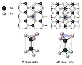 |
| The P and AP phases of a GaSe monolayer CREDIT Hirokazu Nitta from Japan Advanced Institute of Science and Technology |
Abstract:
The gallium selenide monolayer has been recently discovered to have an alternative crystal structure and has diverse potential applications in electronics. Understanding its properties is crucial to understand its functions. Now, scientists from the Japan Advanced Institute of Science and Technology and the University of Tokyo have explored its structural stability, electronic states, and transformation of crystal phases.
Shapeshifting crystals-varying stability in different forms of gallium selenide monolayers: Researchers investigate the structure and properties of a recently identified polymorph of gallium selenide crystal layer
Nomi, Japan | Posted on January 1st, 2021Solid materials comprise a symmetric arrangement of atoms that confer properties like conductivity, strength, and durability. Changes in size can change this arrangement, thereby changing the overall properties of the material. For instance, the electrical, chemical, optical and mechanical properties of certain materials can change as we move towards the "nano" scale. Science now lets us study the differences in properties across various dimensions right from monolayer (atomic) level.
Gallium selenide (GaSe) is a "layered metal-chalcogenide," which is known to have polytypes, which differ in their stacking sequence of layers, but not a polymorph, which has a different atomic arrangement inside the layer. GaSe has sparked a great deal of interest in areas of physical and chemical research, owing to its potential usage in photoconduction, far-infrared conversion, and optical applications. Conventionally, a GaSe monolayer is composed of gallium (Ga) and selenium (Se) atoms bonded covalently, with the Se atoms projecting outwards, forming a trigonal prism-like structure named "P phase." Part of the same research group had earlier reported a novel crystal phase of GaSe using transmission electron microscopy in Surface and Interface Analysis, wherein the Se atoms are arranged in a trigonal antiprismatic manner to the Ga atoms referred to as "AP phase" with a symmetry different from the conventional P phase (see Picture 1). Because of the novelty of this monolayer structure, very little is known about how it does its "shapeshifting." Moreover, how do variations in the intralayer structure of such compounds affect stability?
To answer this, Mr. Hirokazu Nitta and Prof. Yukiko Yamada-Takamura from the Japan Advanced Institute of Science and Technology (JAIST) explored the structural stability and electronic states of phases of GaSe monolayer using first-principles calculations, in their latest study in Physical Review B.
Hirokazu Nitta explains their study, stating, "We have found out through first-principles calculations that this new phase is metastable, and stability against the ground-state conventional phase reverses upon applying tensile strain, which we think is strongly related to the fact that we saw this phase formed only at the film-substrate interface." The published study is also trending as a #PRBTopDownload on the official Physical Review B handle on Twitter: https://twitter.com/PhysRevB/status/1338837972003811331
To compare the structural stability of the P and AP phases of GaSe, the researchers first calculated the total energy at different in-plane lattice constants, which represent the size of a unit cell in the crystal, given that its structure comprises a "lattice" or organized meshwork of atoms. The lowest energy that corresponds to the most stable state was computed and at this state, the P phase was found to be more stable than the AP phase.
Then, to investigate if the AP and P phases can transform into each other, they determined the "energy barriers" that the material needs to cross to change, and additionally performed molecular dynamics calculations using a supercomputer (see Picture 2). They found the energy barrier for phase transition of P-phase and AP-phase GaSe monolayers is large likely due to the need of breaking and making new bonds, which prohibits direct transition from P to AP phase. The calculations also revealed that the relative stability of P-phase and AP-phase GaSe monolayers can be reversed by applying "tensile strain," or a stretching-type force.
Highlighting the importance and future prospects of their study, Prof. Yamada-Takamura remarks, "Layered chalcogenides are interesting 2D materials after graphene, having wide variety and especially bandgap. We have just found out a new polymorph (not polytype) of a layered monochalcogenide. Its physical as well as chemical properties are yet to be discovered."
Together, the findings of this study describe the electronic structure of a less-known structure of GaSe that can provide insights into the behavior of similar epitaxially grown monolayers, revealing yet another secret about the unknown family members of GaSe and related monochalcogenides.
####
About Japan Advanced Institute of Science and Technology (JAIST)
Founded in 1990 in Ishikawa prefecture, the Japan Advanced Institute of Science and Technology (JAIST) was the first independent national graduate school in Japan. Now, after 30 years of steady progress, JAIST has become one of Japan's top-ranking universities. JAIST counts with multiple satellite campuses and strives to foster capable leaders with a state-of-the-art education system where diversity is key; about 40% of its alumni are international students. The university has a unique style of graduate education based on a carefully designed coursework-oriented curriculum to ensure that its students have a solid foundation on which to carry out cutting-edge research. JAIST also works closely both with local and overseas communities by promoting industry-academia collaborative research.
About Professor Yukiko Yamada-Takamura from Japan Advanced Institute of Science and Technology, Japan
Dr. Yukiko Yamada-Takamura is a Professor in the School of Materials Science at the Japan Advanced Institute of Science and Technology (JAIST), Japan, since 2020. She received her PhD from the University of Tokyo in 1998. She was a research associate at Tohoku University from 2002-2006. She joined JAIST as a lecturer in 2006. She specializes in material fabrication and microstructure control, nanostructure physics and nanomaterials. Her research interest lies in thin films, 2D materials, and cutting-edge microscopies.
For more information, please click here
Contacts:
Yukiko Yamada-Takamura
81-076-151-1570
Copyright © Japan Advanced Institute of Science and Technology (JAIST)
If you have a comment, please Contact us.Issuers of news releases, not 7th Wave, Inc. or Nanotechnology Now, are solely responsible for the accuracy of the content.
Bookmark:


| Related Links |
| Related News Press |
News and information
![]() Researchers develop molecular qubits that communicate at telecom frequencies October 3rd, 2025
Researchers develop molecular qubits that communicate at telecom frequencies October 3rd, 2025
![]() Next-generation quantum communication October 3rd, 2025
Next-generation quantum communication October 3rd, 2025
![]() "Nanoreactor" cage uses visible light for catalytic and ultra-selective cross-cycloadditions October 3rd, 2025
"Nanoreactor" cage uses visible light for catalytic and ultra-selective cross-cycloadditions October 3rd, 2025
Possible Futures
![]() Spinel-type sulfide semiconductors to operate the next-generation LEDs and solar cells For solar-cell absorbers and green-LED source October 3rd, 2025
Spinel-type sulfide semiconductors to operate the next-generation LEDs and solar cells For solar-cell absorbers and green-LED source October 3rd, 2025
Chip Technology
![]() Lab to industry: InSe wafer-scale breakthrough for future electronics August 8th, 2025
Lab to industry: InSe wafer-scale breakthrough for future electronics August 8th, 2025
![]() A 1960s idea inspires NBI researchers to study hitherto inaccessible quantum states June 6th, 2025
A 1960s idea inspires NBI researchers to study hitherto inaccessible quantum states June 6th, 2025
![]() Programmable electron-induced color router array May 14th, 2025
Programmable electron-induced color router array May 14th, 2025
Nanoelectronics
![]() Lab to industry: InSe wafer-scale breakthrough for future electronics August 8th, 2025
Lab to industry: InSe wafer-scale breakthrough for future electronics August 8th, 2025
![]() Interdisciplinary: Rice team tackles the future of semiconductors Multiferroics could be the key to ultralow-energy computing October 6th, 2023
Interdisciplinary: Rice team tackles the future of semiconductors Multiferroics could be the key to ultralow-energy computing October 6th, 2023
![]() Key element for a scalable quantum computer: Physicists from Forschungszentrum J�lich and RWTH Aachen University demonstrate electron transport on a quantum chip September 23rd, 2022
Key element for a scalable quantum computer: Physicists from Forschungszentrum J�lich and RWTH Aachen University demonstrate electron transport on a quantum chip September 23rd, 2022
![]() Reduced power consumption in semiconductor devices September 23rd, 2022
Reduced power consumption in semiconductor devices September 23rd, 2022
Discoveries
![]() Researchers develop molecular qubits that communicate at telecom frequencies October 3rd, 2025
Researchers develop molecular qubits that communicate at telecom frequencies October 3rd, 2025
![]() Next-generation quantum communication October 3rd, 2025
Next-generation quantum communication October 3rd, 2025
![]() "Nanoreactor" cage uses visible light for catalytic and ultra-selective cross-cycloadditions October 3rd, 2025
"Nanoreactor" cage uses visible light for catalytic and ultra-selective cross-cycloadditions October 3rd, 2025
Announcements
![]() Rice membrane extracts lithium from brines with greater speed, less waste October 3rd, 2025
Rice membrane extracts lithium from brines with greater speed, less waste October 3rd, 2025
![]() Researchers develop molecular qubits that communicate at telecom frequencies October 3rd, 2025
Researchers develop molecular qubits that communicate at telecom frequencies October 3rd, 2025
![]() Next-generation quantum communication October 3rd, 2025
Next-generation quantum communication October 3rd, 2025
![]() "Nanoreactor" cage uses visible light for catalytic and ultra-selective cross-cycloadditions October 3rd, 2025
"Nanoreactor" cage uses visible light for catalytic and ultra-selective cross-cycloadditions October 3rd, 2025
Interviews/Book Reviews/Essays/Reports/Podcasts/Journals/White papers/Posters
![]() Spinel-type sulfide semiconductors to operate the next-generation LEDs and solar cells For solar-cell absorbers and green-LED source October 3rd, 2025
Spinel-type sulfide semiconductors to operate the next-generation LEDs and solar cells For solar-cell absorbers and green-LED source October 3rd, 2025
![]() Rice membrane extracts lithium from brines with greater speed, less waste October 3rd, 2025
Rice membrane extracts lithium from brines with greater speed, less waste October 3rd, 2025
|
|
||
|
|
||
| The latest news from around the world, FREE | ||
|
|
||
|
|
||
| Premium Products | ||
|
|
||
|
Only the news you want to read!
Learn More |
||
|
|
||
|
Full-service, expert consulting
Learn More |
||
|
|
||