Home > Press > Atomic-scale nanowires can now be produced at scale: Scalable synthesis of transition metal chalcogenide nanowires for next-gen electronics
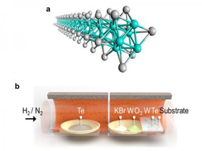 |
| (a) Illustration of a TMC nanowire (b) Chemical vapor deposition. The ingredients are vaporized in a hydrogen/nitrogen atmosphere and allowed to deposit and self-assemble on a substrate. Reprinted with permission from Ref. 1 CREDIT Copyright 2020 American Chemical Society (ACS) |
Abstract:
Researchers from Tokyo Metropolitan University have discovered a way to make self-assembled nanowires of transition metal chalcogenides at scale using chemical vapor deposition. By changing the substrate where the wires form, they can tune how these wires are arranged, from aligned configurations of atomically thin sheets to random networks of bundles. This paves the way to industrial deployment in next-gen industrial electronics, including energy harvesting, and transparent, efficient, even flexible devices.
Atomic-scale nanowires can now be produced at scale: Scalable synthesis of transition metal chalcogenide nanowires for next-gen electronics
Tokyo, Japan | Posted on December 25th, 2020Electronics is all about making things smaller. Smaller features on a chip, for example, means more computing power in the same amount of space and better efficiency, essential to feeding the increasingly heavy demands of a modern IT infrastructure powered by machine learning and artificial intelligence. And as devices get smaller, the same demands are made of the intricate wiring that ties everything together. The ultimate goal would be a wire that is only an atom or two in thickness. Such nanowires would begin to leverage completely different physics as the electrons that travel through them behave more and more as if they live in a one-dimensional world, not a 3D one.
In fact, scientists already have materials like carbon nanotubes and transition metal chalcogenides (TMCs), mixtures of transition metals and group 16 elements which can self-assemble into atomic-scale nanowires. The trouble is making them long enough, and at scale. A way to mass produce nanowires would be a game changer.
Now, a team led by Dr. Hong En Lim and Associate Professor Yasumitsu Miyata from Tokyo Metropolitan University has come up with a way of making long wires of transition metal telluride nanowires at unprecedentedly large scales. Using a process called chemical vapor deposition (CVD), they found that they could assemble TMC nanowires in different arrangements depending on the surface or substrate that they use as a template. Examples are shown in Figure 2; in (a), nanowires grown on a silicon/silica substrate form a random network of bundles; in (b), the wires assemble in a set direction on a sapphire substrate, following the structure of the underlying sapphire crystal. By simply changing where they are grown, the team now have access to centimeter-sized wafers covered in the arrangement they desired, including monolayers, bilayers and networks of bundles, all with different applications. They also found that the structure of the wires themselves were highly crystalline and ordered, and that their properties, including their excellent conductivity and 1D-like behavior, matched those found in theoretical predictions.
Having large amounts of long, highly crystalline nanowires is sure to help physicists characterize and study these exotic structures in more depth. Importantly, it's an exciting step towards seeing real-world applications of atomically-thin wires, in transparent and flexible electronics, ultra-efficient devices and energy harvesting applications.
This work was supported by JST CREST Grants (JPMJCR16F3, JPMJCR17I5), Japan Society for the Promotion of Science (JSPS) KAKENHI Grants-in-Aid for Scientific Research (B) (JP18H01832, JP19H02543, JP20H02572, JP20H02573), Young Scientists (JP19K15383, JP19K15393), Scientific Research on Innovative Areas (JP20H05189, JP26102012), Specially Promoted Research (JP25000003), Challenging Research (Exploratory) (19K22127), and Scientific Research (A) (JP17H01069), and grants from the Murata Science Foundation (2019, H31-068) and the Japan Keirin Autorace Foundation (2020M-121). This work was partially conducted at the AIST Nano-Processing Facility supported by "Nanotechnology Platform Program" of the Ministry of Education, Culture, Sports, Science and Technology (MEXT), Japan. Grant Number JPMXP09F19008709 and 20009034.
####
For more information, please click here
Contacts:
Go Totsukawa
81-426-772-728
@TMU_PR
Copyright © Tokyo Metropolitan University
If you have a comment, please Contact us.Issuers of news releases, not 7th Wave, Inc. or Nanotechnology Now, are solely responsible for the accuracy of the content.
Bookmark:


| Related Links |
| Related News Press |
News and information
![]() Quantum computer improves AI predictions April 17th, 2026
Quantum computer improves AI predictions April 17th, 2026
![]() Flexible sensor gains sensitivity under pressure April 17th, 2026
Flexible sensor gains sensitivity under pressure April 17th, 2026
![]() A reusable chip for particulate matter sensing April 17th, 2026
A reusable chip for particulate matter sensing April 17th, 2026
![]() Detecting vibrational quantum beating in the predissociation dynamics of SF6 using time-resolved photoelectron spectroscopy April 17th, 2026
Detecting vibrational quantum beating in the predissociation dynamics of SF6 using time-resolved photoelectron spectroscopy April 17th, 2026
Govt.-Legislation/Regulation/Funding/Policy
![]() Quantum computer improves AI predictions April 17th, 2026
Quantum computer improves AI predictions April 17th, 2026
![]() Metasurfaces smooth light to boost magnetic sensing precision January 30th, 2026
Metasurfaces smooth light to boost magnetic sensing precision January 30th, 2026
![]() New imaging approach transforms study of bacterial biofilms August 8th, 2025
New imaging approach transforms study of bacterial biofilms August 8th, 2025
Possible Futures
![]() A fundamentally new therapeutic approach to cystic fibrosis: Nanobody repairs cellular defect April 17th, 2026
A fundamentally new therapeutic approach to cystic fibrosis: Nanobody repairs cellular defect April 17th, 2026
![]() UC Irvine physicists discover method to reverse �quantum scrambling� : The work addresses the problem of information loss in quantum computing system April 17th, 2026
UC Irvine physicists discover method to reverse �quantum scrambling� : The work addresses the problem of information loss in quantum computing system April 17th, 2026
Chip Technology
![]() A reusable chip for particulate matter sensing April 17th, 2026
A reusable chip for particulate matter sensing April 17th, 2026
![]() Metasurfaces smooth light to boost magnetic sensing precision January 30th, 2026
Metasurfaces smooth light to boost magnetic sensing precision January 30th, 2026
Self Assembly
![]() Diamond glitter: A play of colors with artificial DNA crystals May 17th, 2024
Diamond glitter: A play of colors with artificial DNA crystals May 17th, 2024
![]() Liquid crystal templated chiral nanomaterials October 14th, 2022
Liquid crystal templated chiral nanomaterials October 14th, 2022
![]() Nanoclusters self-organize into centimeter-scale hierarchical assemblies April 22nd, 2022
Nanoclusters self-organize into centimeter-scale hierarchical assemblies April 22nd, 2022
![]() Atom by atom: building precise smaller nanoparticles with templates March 4th, 2022
Atom by atom: building precise smaller nanoparticles with templates March 4th, 2022
Nanoelectronics
![]() Lab to industry: InSe wafer-scale breakthrough for future electronics August 8th, 2025
Lab to industry: InSe wafer-scale breakthrough for future electronics August 8th, 2025
![]() Interdisciplinary: Rice team tackles the future of semiconductors Multiferroics could be the key to ultralow-energy computing October 6th, 2023
Interdisciplinary: Rice team tackles the future of semiconductors Multiferroics could be the key to ultralow-energy computing October 6th, 2023
![]() Key element for a scalable quantum computer: Physicists from Forschungszentrum J�lich and RWTH Aachen University demonstrate electron transport on a quantum chip September 23rd, 2022
Key element for a scalable quantum computer: Physicists from Forschungszentrum J�lich and RWTH Aachen University demonstrate electron transport on a quantum chip September 23rd, 2022
![]() Reduced power consumption in semiconductor devices September 23rd, 2022
Reduced power consumption in semiconductor devices September 23rd, 2022
Discoveries
![]() Quantum computer improves AI predictions April 17th, 2026
Quantum computer improves AI predictions April 17th, 2026
![]() Flexible sensor gains sensitivity under pressure April 17th, 2026
Flexible sensor gains sensitivity under pressure April 17th, 2026
![]() A reusable chip for particulate matter sensing April 17th, 2026
A reusable chip for particulate matter sensing April 17th, 2026
![]() Detecting vibrational quantum beating in the predissociation dynamics of SF6 using time-resolved photoelectron spectroscopy April 17th, 2026
Detecting vibrational quantum beating in the predissociation dynamics of SF6 using time-resolved photoelectron spectroscopy April 17th, 2026
Announcements
![]() A fundamentally new therapeutic approach to cystic fibrosis: Nanobody repairs cellular defect April 17th, 2026
A fundamentally new therapeutic approach to cystic fibrosis: Nanobody repairs cellular defect April 17th, 2026
![]() UC Irvine physicists discover method to reverse �quantum scrambling� : The work addresses the problem of information loss in quantum computing system April 17th, 2026
UC Irvine physicists discover method to reverse �quantum scrambling� : The work addresses the problem of information loss in quantum computing system April 17th, 2026
Interviews/Book Reviews/Essays/Reports/Podcasts/Journals/White papers/Posters
![]() A fundamentally new therapeutic approach to cystic fibrosis: Nanobody repairs cellular defect April 17th, 2026
A fundamentally new therapeutic approach to cystic fibrosis: Nanobody repairs cellular defect April 17th, 2026
![]() UC Irvine physicists discover method to reverse �quantum scrambling� : The work addresses the problem of information loss in quantum computing system April 17th, 2026
UC Irvine physicists discover method to reverse �quantum scrambling� : The work addresses the problem of information loss in quantum computing system April 17th, 2026
Grants/Sponsored Research/Awards/Scholarships/Gifts/Contests/Honors/Records
![]() Quantum computer improves AI predictions April 17th, 2026
Quantum computer improves AI predictions April 17th, 2026
![]() Detecting vibrational quantum beating in the predissociation dynamics of SF6 using time-resolved photoelectron spectroscopy April 17th, 2026
Detecting vibrational quantum beating in the predissociation dynamics of SF6 using time-resolved photoelectron spectroscopy April 17th, 2026
![]() Metasurfaces smooth light to boost magnetic sensing precision January 30th, 2026
Metasurfaces smooth light to boost magnetic sensing precision January 30th, 2026
|
|
||
|
|
||
| The latest news from around the world, FREE | ||
|
|
||
|
|
||
| Premium Products | ||
|
|
||
|
Only the news you want to read!
Learn More |
||
|
|
||
|
Full-service, expert consulting
Learn More |
||
|
|
||