Home > Press > Aledia, French Developer of Next-Generation MicroLED Displays For High-Volume Consumer Markets, Announces it Has Produced its First Nanowire Chips on 300mm Silicon Wafers Using CEA-Leti Pilot Lines: Company will produce microLEDs on both 200mm and 300mm silicon wafers
 |
Abstract:
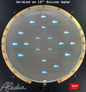
Aledia, a French startup pioneering a disruptive technology for microLED displays, today announced it has manufactured the world’s first microLED chips produced on 300mm (12”) silicon wafers. The company, which developed its breakthrough technology on 200mm (8”) silicon wafers over the past eight years, will produce the chips on both 200mm and 300mm wafers. The larger wafers provide better economic payoff and cost-effective integration with smaller-node electronics, which are only available on 300mm silicon wafers. Aledia was spun out of CEA-Leti, a French research institute pioneering micro- and nanotechnologies, in 2012, and the work on 300mm wafers has been performed by joint Aledia and CEA-Leti teams.
Aledia, French Developer of Next-Generation MicroLED Displays For High-Volume Consumer Markets, Announces it Has Produced its First Nanowire Chips on 300mm Silicon Wafers Using CEA-Leti Pilot Lines: Company will produce microLEDs on both 200mm and 300mm silicon wafers
Echirolles, France | Posted on December 15th, 2020“We believe producing microLEDs on large-area 300mm silicon wafers is a world’s first, and opens this technology to huge potential-volume-manufacturing capabilities,” said Giorgio Anania, Aledia CEO and cofounder. “The larger size allows 60-100 smartphone displays to be made on a single 300mm wafer, versus approximately four-to-six using the present LED industry-standard, 4” sapphire substrate. Thanks to Aledia’s unique nanowire LED technology (3D LED), this can be done with commercially available processes and equipment, since it uses standard-thickness (780µm) silicon wafers.”
Traditional planar, “2D” microLEDs are produced by depositing flat layers of gallium-nitride (GaN) crystal on sapphire wafers of 100-150mm diameter (4-6”), with the majority of production today being on 100mm (4”) wafers. Aledia’s microLED technology grows GaN nanowires (GaN crystals of sub-micron diameter) on top of large-area silicon (called “3D”). This 3D nanowire technology does not create any of the stresses seen on 2D chips, which build up as the wafer size is increased, and so allows the use of very large-size wafers. In addition, this silicon-based technology allows production in conventional microelectronics fabs, called silicon foundries, which can be ramped up to high volume production with extremely high yield.
“We are very pleased to have helped Aledia push forward the state of the art of 3D LED manufacturing using our 300mm silicon processing line. We believe large-area silicon wafers are the best manufacturing platform in the world today for displays, and give big advantages in manufacturability,” said Emmanuel Sabonnadičre, CEO of CEA-Leti. “3D nanowire micro-LEDs have the potential to make serious penetration into large display markets. CEA-Leti is very active today in supporting the display industry’s transition to micro-LED technology.”
“We believe the use of large-area silicon wafers and microelectronics foundries are the only way to deliver the huge volumes demanded by end-user markets,” Anania said. “For example, if only the large-screen TVs of 60” in diagonal and larger transitioned to silicon nanowire technology to obtain better image quality and lower manufacturing costs, this would require 24 million 300mm wafers per year, volumes that can only be delivered by the silicon industry and supply chains. Smartphones, laptops and tablets would be on top of that.”
Aledia’s technology is protected by 197 patent families, making Aledia the leading French startup company in France in filed patents.
This work is sponsored by the EC: Grant Agreement number: 954553 — SPEED — H2020-EIC-SMEInst-2018-2020
####
About CEA Leti
Leti, a technology research institute at CEA, is a global leader in miniaturization technologies enabling smart, energy-efficient and secure solutions for industry. CEA-Leti pioneers micro and nanotechnologies, tailoring differentiating applicative solutions for global companies, SMEs and startups. CEA-Leti tackles critical challenges in healthcare, energy and digital migration. From sensors to data processing and computing solutions, CEA-Leti’s multidisciplinary teams deliver solid expertise, leveraging world-class pre-industrialization facilities. With a staff of more than 1,900, a portfolio of 3,100 patents, 10,000 sq. meters of cleanroom space and a clear IP policy, the institute is based in Grenoble, France, and has offices in Silicon Valley and Tokyo. CEA-Leti has launched 65 startups and is a member of the Carnot Institutes network. Follow us on www.leti-cea.com and @CEA_Leti. CEA. For more information: www.cea.fr/english
About Aledia
Aledia develops and manufactures microLED displays and components to equip the $120 billion worldwide display market with next-generation technology. Its proprietary 3D microLED technology uses GaN nanowires on large-area silicon that emit light and can be used to manufacture state-of-the-art displays that deliver better performance at competitive prices compared to current OLED technologies. These improvements include longer battery life on mobile devices, better outdoor readability and faster refresh rates, as well as sharper colors. The company is targeting markets for smartphones, laptops and tablets, augmented reality displays and large TVs. Based in the Grenoble area in France, Aledia has 130 employees. It was spun out of CEA-Leti, the French microelectronics R&D institute, in 2012. Visit www.aledia.com/
For more information, please click here
Contacts:
Press Contact
Sarah-Lyle Dampoux
+33 (0) 6 74 93 23 47
Copyright © CEA Leti
If you have a comment, please Contact us.Issuers of news releases, not 7th Wave, Inc. or Nanotechnology Now, are solely responsible for the accuracy of the content.
Bookmark:


| Related News Press |
News and information
![]() Quantum computer improves AI predictions April 17th, 2026
Quantum computer improves AI predictions April 17th, 2026
![]() Flexible sensor gains sensitivity under pressure April 17th, 2026
Flexible sensor gains sensitivity under pressure April 17th, 2026
![]() A reusable chip for particulate matter sensing April 17th, 2026
A reusable chip for particulate matter sensing April 17th, 2026
![]() Detecting vibrational quantum beating in the predissociation dynamics of SF6 using time-resolved photoelectron spectroscopy April 17th, 2026
Detecting vibrational quantum beating in the predissociation dynamics of SF6 using time-resolved photoelectron spectroscopy April 17th, 2026
Display technology/LEDs/SS Lighting/OLEDs
![]() Spinel-type sulfide semiconductors to operate the next-generation LEDs and solar cells For solar-cell absorbers and green-LED source October 3rd, 2025
Spinel-type sulfide semiconductors to operate the next-generation LEDs and solar cells For solar-cell absorbers and green-LED source October 3rd, 2025
![]() Efficient and stable hybrid perovskite-organic light-emitting diodes with external quantum efficiency exceeding 40 per cent July 5th, 2024
Efficient and stable hybrid perovskite-organic light-emitting diodes with external quantum efficiency exceeding 40 per cent July 5th, 2024
Possible Futures
![]() A fundamentally new therapeutic approach to cystic fibrosis: Nanobody repairs cellular defect April 17th, 2026
A fundamentally new therapeutic approach to cystic fibrosis: Nanobody repairs cellular defect April 17th, 2026
![]() UC Irvine physicists discover method to reverse ‘quantum scrambling’ : The work addresses the problem of information loss in quantum computing system April 17th, 2026
UC Irvine physicists discover method to reverse ‘quantum scrambling’ : The work addresses the problem of information loss in quantum computing system April 17th, 2026
Chip Technology
![]() A reusable chip for particulate matter sensing April 17th, 2026
A reusable chip for particulate matter sensing April 17th, 2026
![]() Metasurfaces smooth light to boost magnetic sensing precision January 30th, 2026
Metasurfaces smooth light to boost magnetic sensing precision January 30th, 2026
Nanoelectronics
![]() Lab to industry: InSe wafer-scale breakthrough for future electronics August 8th, 2025
Lab to industry: InSe wafer-scale breakthrough for future electronics August 8th, 2025
![]() Interdisciplinary: Rice team tackles the future of semiconductors Multiferroics could be the key to ultralow-energy computing October 6th, 2023
Interdisciplinary: Rice team tackles the future of semiconductors Multiferroics could be the key to ultralow-energy computing October 6th, 2023
![]() Key element for a scalable quantum computer: Physicists from Forschungszentrum Jülich and RWTH Aachen University demonstrate electron transport on a quantum chip September 23rd, 2022
Key element for a scalable quantum computer: Physicists from Forschungszentrum Jülich and RWTH Aachen University demonstrate electron transport on a quantum chip September 23rd, 2022
![]() Reduced power consumption in semiconductor devices September 23rd, 2022
Reduced power consumption in semiconductor devices September 23rd, 2022
Announcements
![]() A fundamentally new therapeutic approach to cystic fibrosis: Nanobody repairs cellular defect April 17th, 2026
A fundamentally new therapeutic approach to cystic fibrosis: Nanobody repairs cellular defect April 17th, 2026
![]() UC Irvine physicists discover method to reverse ‘quantum scrambling’ : The work addresses the problem of information loss in quantum computing system April 17th, 2026
UC Irvine physicists discover method to reverse ‘quantum scrambling’ : The work addresses the problem of information loss in quantum computing system April 17th, 2026
Research partnerships
![]() Lab to industry: InSe wafer-scale breakthrough for future electronics August 8th, 2025
Lab to industry: InSe wafer-scale breakthrough for future electronics August 8th, 2025
![]() HKU physicists uncover hidden order in the quantum world through deconfined quantum critical points April 25th, 2025
HKU physicists uncover hidden order in the quantum world through deconfined quantum critical points April 25th, 2025
|
|
||
|
|
||
| The latest news from around the world, FREE | ||
|
|
||
|
|
||
| Premium Products | ||
|
|
||
|
Only the news you want to read!
Learn More |
||
|
|
||
|
Full-service, expert consulting
Learn More |
||
|
|
||