Home > Press > Sticker makes nanoscale light manipulation easier to manufacture
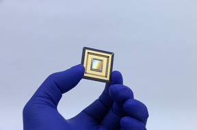 |
| Researchers have given sensors the ability to manipulate light better, thanks to a sticker in the center of this device. (Purdue University image/Bongjoong Kim) |
Abstract:
Deterministic Nanoassembly of Quasi-Three-Dimensional Plasmonic Nanoarrays with Arbitrary Substrate Materials and Structures
Bongjoong Kim,† Jiyeon Jeon,‡ Yue Zhang,§ Dae Seung Wie,† Jehwan Hwang,‡ Sang Jun Lee,‡ Dennis E. Walker, Jr.,∥ Don C. Abeysinghe,⊥ Augustine Urbas,⊥ Baoxing Xu,*,§ Zahyun Ku,*,⊥ and Chi Hwan Lee*,†,#,∇
† School of Mechanical Engineering, Purdue University, West Lafayette, Indiana, United States
‡ Division of Industrial Metrology, Korea Research Institute of Standards and Science, Daejeon, Korea
Department of Mechanical and Aerospace Engineering, University of Virginia, Charlottesville, Virginia, United States
∥ Sensors Directorate, Air Force Research Laboratory, Wright-Patterson AFB, United States
⊥Materials and Manufacturing Directorate, Air Force Research Laboratory, Wright-Patterson AFB, United States
#Weldon School of Biomedical Engineering, Purdue University, West Lafayette, Indiana, United States
∇Department of Speech, Language, and Hearing Sciences, Purdue University, West Lafayette, Indiana, United States
DOI: 10.1021/acs.nanolett.9b02598
Guided manipulation of light through periodic nanoarrays of three-dimensional (3D) metal–dielectric patterns provides remarkable opportunities to harness light in a way that cannot be obtained with conventional optics yet its practical implementation remains hindered by a lack of effective methodology. Here we report a novel 3D nanoassembly method that enables deterministic integration of quasi-3D plasmonic nanoarrays with a foreign substrate composed of arbitrary materials and structures. This method is versatile to arrange a variety of types of metal–dielectric composite nanoarrays in lateral and vertical configurations, providing a route to generate heterogeneous material compositions, complex device layouts, and tailored functionalities. Experimental, computational, and theoretical studies reveal the essential design features of this approach and, taken together with implementation of automated equipment, provide a technical guidance for large-scale manufacturability. Pilot assembly of specifically engineered quasi-3D plasmonic nanoarrays with a model hybrid pixel detector for deterministic enhancement of the detection performances demonstrates the utility of this method.
Sticker makes nanoscale light manipulation easier to manufacture
West Lafayette, IN | Posted on August 27th, 2019Human pathogens, such as HIV and viruses causing respiratory tract infection, have molecular fingerprints that are difficult to distinguish. To better detect these pathogens, sensors in diagnostic tools need to manipulate light on a nanoscale.
But there isn’t a good way to manufacture these light manipulation devices without damaging the sensors. Purdue University engineers have a solution: Stickers.
In a paper published in Nano Letters, the team integrated light manipulation devices called 3D plasmonic nanoarrays onto peelable films that can stick to any surface. They tested the sticker-nanoarray’s capabilities on the lenses of sensors, which make up conventional imaging systems.
The Air Force Research Laboratory supported the work and validated the sticker’s performance and properties.
“Unlike any existing approaches, the entire process occurs in distilled water at room temperature without the chemical, thermal or mechanical treatments that can damage sensitive surfaces, such as a sensor lens,” said Chi Hwan Lee, an assistant professor of biomedical engineering and mechanical engineering at Purdue.
To turn the nanoarrays into a sticker, the researchers built them into a film on a silicon wafer. When submerged in distilled water, the film peels cleanly from the wafer, allowing the wafer to be reused. The film can then stick to the desired surface without damaging it.
“Because this methodology allows 3D plasmonic nanoarrays to physically separate from a donor wafer and transfer over to another surface without defect, it offers a major cost- and time-saving factor in the manufacturing scheme,” Lee said.
The researchers also demonstrated that the process works for various classes of 3D plasmonic nanoarrays in both lateral and vertical configurations, offering more functionality.
Lee’s lab plans to further develop these sticker-nanoarrays for biological sensing applications, such as for protein detection in clinical diagnostics. The lab has already created electronic stickers that serve as bio-patches for drug delivery. They also can enable ordinary objects to wirelessly connect to a network, creating an “Internet of Things.”
The method has been patented via the Purdue Research Foundation Office of Technology Commercialization. This research aligns with Purdue's Giant Leaps celebration, acknowledging the university’s global advancements made in health, longevity and quality of life as part of Purdue’s 150th anniversary. This is one of the four themes of the yearlong celebration’s Ideas Festival, designed to showcase Purdue as an intellectual center solving real-world issues.
####
For more information, please click here
Contacts:
Writer: Kayla Wiles, 765-494-2432,
Source: Chi Hwan Lee, 765-494-6212,
Copyright © Purdue University
If you have a comment, please Contact us.Issuers of news releases, not 7th Wave, Inc. or Nanotechnology Now, are solely responsible for the accuracy of the content.
Bookmark:


| Related News Press |
News and information
![]() Simulating magnetization in a Heisenberg quantum spin chain April 5th, 2024
Simulating magnetization in a Heisenberg quantum spin chain April 5th, 2024
![]() NRL charters Navy’s quantum inertial navigation path to reduce drift April 5th, 2024
NRL charters Navy’s quantum inertial navigation path to reduce drift April 5th, 2024
![]() Discovery points path to flash-like memory for storing qubits: Rice find could hasten development of nonvolatile quantum memory April 5th, 2024
Discovery points path to flash-like memory for storing qubits: Rice find could hasten development of nonvolatile quantum memory April 5th, 2024
Imaging
![]() Nanoscale CL thermometry with lanthanide-doped heavy-metal oxide in TEM March 8th, 2024
Nanoscale CL thermometry with lanthanide-doped heavy-metal oxide in TEM March 8th, 2024
![]() The USTC realizes In situ electron paramagnetic resonance spectroscopy using single nanodiamond sensors November 3rd, 2023
The USTC realizes In situ electron paramagnetic resonance spectroscopy using single nanodiamond sensors November 3rd, 2023
![]() Observation of left and right at nanoscale with optical force October 6th, 2023
Observation of left and right at nanoscale with optical force October 6th, 2023
Internet-of-Things
![]() New nanowire sensors are the next step in the Internet of Things January 6th, 2023
New nanowire sensors are the next step in the Internet of Things January 6th, 2023
![]() New chip ramps up AI computing efficiency August 19th, 2022
New chip ramps up AI computing efficiency August 19th, 2022
![]() Lightening up the nanoscale long-wavelength optoelectronics May 13th, 2022
Lightening up the nanoscale long-wavelength optoelectronics May 13th, 2022
![]() Thin-film, high-frequency antenna array offers new flexibility for wireless communications November 5th, 2021
Thin-film, high-frequency antenna array offers new flexibility for wireless communications November 5th, 2021
Possible Futures
![]() Discovery points path to flash-like memory for storing qubits: Rice find could hasten development of nonvolatile quantum memory April 5th, 2024
Discovery points path to flash-like memory for storing qubits: Rice find could hasten development of nonvolatile quantum memory April 5th, 2024
![]() With VECSELs towards the quantum internet Fraunhofer: IAF achieves record output power with VECSEL for quantum frequency converters April 5th, 2024
With VECSELs towards the quantum internet Fraunhofer: IAF achieves record output power with VECSEL for quantum frequency converters April 5th, 2024
Nanomedicine
![]() New micromaterial releases nanoparticles that selectively destroy cancer cells April 5th, 2024
New micromaterial releases nanoparticles that selectively destroy cancer cells April 5th, 2024
![]() Good as gold - improving infectious disease testing with gold nanoparticles April 5th, 2024
Good as gold - improving infectious disease testing with gold nanoparticles April 5th, 2024
![]() Researchers develop artificial building blocks of life March 8th, 2024
Researchers develop artificial building blocks of life March 8th, 2024
Sensors
Discoveries
![]() Chemical reactions can scramble quantum information as well as black holes April 5th, 2024
Chemical reactions can scramble quantum information as well as black holes April 5th, 2024
![]() New micromaterial releases nanoparticles that selectively destroy cancer cells April 5th, 2024
New micromaterial releases nanoparticles that selectively destroy cancer cells April 5th, 2024
![]() Utilizing palladium for addressing contact issues of buried oxide thin film transistors April 5th, 2024
Utilizing palladium for addressing contact issues of buried oxide thin film transistors April 5th, 2024
Announcements
![]() NRL charters Navy’s quantum inertial navigation path to reduce drift April 5th, 2024
NRL charters Navy’s quantum inertial navigation path to reduce drift April 5th, 2024
![]() Discovery points path to flash-like memory for storing qubits: Rice find could hasten development of nonvolatile quantum memory April 5th, 2024
Discovery points path to flash-like memory for storing qubits: Rice find could hasten development of nonvolatile quantum memory April 5th, 2024
Interviews/Book Reviews/Essays/Reports/Podcasts/Journals/White papers/Posters
![]() Simulating magnetization in a Heisenberg quantum spin chain April 5th, 2024
Simulating magnetization in a Heisenberg quantum spin chain April 5th, 2024
![]() Discovery points path to flash-like memory for storing qubits: Rice find could hasten development of nonvolatile quantum memory April 5th, 2024
Discovery points path to flash-like memory for storing qubits: Rice find could hasten development of nonvolatile quantum memory April 5th, 2024
Nanobiotechnology
![]() New micromaterial releases nanoparticles that selectively destroy cancer cells April 5th, 2024
New micromaterial releases nanoparticles that selectively destroy cancer cells April 5th, 2024
![]() Good as gold - improving infectious disease testing with gold nanoparticles April 5th, 2024
Good as gold - improving infectious disease testing with gold nanoparticles April 5th, 2024
![]() Researchers develop artificial building blocks of life March 8th, 2024
Researchers develop artificial building blocks of life March 8th, 2024
|
|
||
|
|
||
| The latest news from around the world, FREE | ||
|
|
||
|
|
||
| Premium Products | ||
|
|
||
|
Only the news you want to read!
Learn More |
||
|
|
||
|
Full-service, expert consulting
Learn More |
||
|
|
||