Home > Press > The moirť patterns of three layers change the electronic properties of graphene
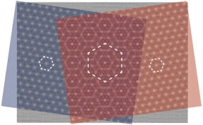 |
| A graphene layer (black) of hexagonally arranged carbon atoms is placed between two layers of boron nitride atoms, which are also arranged hexagonally with a slightly different size. The overlap creates honeycomb patterns in various sizes. CREDIT Swiss Nanoscience Institute, University of Basel |
Abstract:
Combining an atomically thin graphene and a boron nitride layer at a slightly rotated angle changes their electrical properties. Physicists at the University of Basel have now shown for the first time the combination with a third layer can result in new material properties also in a three-layer sandwich of carbon and boron nitride. This significantly increases the number of potential synthetic materials, report the researchers in the scientific journal Nano Letters.
The moirť patterns of three layers change the electronic properties of graphene
Basel, Switzerland | Posted on March 8th, 2019Last year, researchers in the US caused a big stir when they showed that rotating two stacked graphene layers by a "magical" angle of 1.1 degrees turns graphene superconducting - a striking example of how the combination of atomically thin materials can produce completely new electrical properties.
Precision alignment
Scientists from the Swiss Nanoscience Institute and the Department of Physics at the University of Basel have now taken this concept one step further. They placed a layer of graphene between two boron nitride layers, which is often serves to protect the sensitive carbon structure. Doing so, they aligned the layers very precisely with the crystal lattice of the graphene.
The effect observed by the physicists in Professor Christian SchŲnenberger's team is commonly known as a moirť pattern: when two regular patterns are superimposed, a new pattern results with a larger periodic lattice.
New three-layer superlattice
Lujun Wang, a member of the SNI PhD School and researcher in SchŲnenberger's team, also observed effects of this kind of superlattice when he combined layers of boron nitride and graphene. The atoms are arranged hexagonally in all layers. If they are stacked on top of each other, larger regular patterns emerge, with a size depending on the angle between the layers.
It had already been shown that this works with a two-layer combination of graphene and boron nitride, but the effects due to a second boron nitride layer had not yet been found.
When the physicists from Basel experimented with three layers, two superlattices were formed between the graphene and the upper and the lower boron nitride layer, respectively. The superposition of all three layers created an even larger superstructure than possible with only one layer.
Scientists are very interested in these types of synthetic materials, since the different moirť patterns can be used to change or artificially produce new electronic material properties.
"To put it simply, the atomic patterns determine the behavior of electrons in a material, and we are combining different naturally occurring patterns to create new synthetic materials," explains Dr. Andreas Baumgartner, who supervised the project. "Now we have discovered effects in these tailor-made electronic devices that are consistent with a three-layer superstructure," he adds.
####
For more information, please click here
Contacts:
Ylenia Sartorel
@UniBasel_en
Copyright © University of Basel
If you have a comment, please Contact us.Issuers of news releases, not 7th Wave, Inc. or Nanotechnology Now, are solely responsible for the accuracy of the content.
Bookmark:


| Related Links |
| Related News Press |
News and information
![]() Simulating magnetization in a Heisenberg quantum spin chain April 5th, 2024
Simulating magnetization in a Heisenberg quantum spin chain April 5th, 2024
![]() NRL charters Navyís quantum inertial navigation path to reduce drift April 5th, 2024
NRL charters Navyís quantum inertial navigation path to reduce drift April 5th, 2024
![]() Discovery points path to flash-like memory for storing qubits: Rice find could hasten development of nonvolatile quantum memory April 5th, 2024
Discovery points path to flash-like memory for storing qubits: Rice find could hasten development of nonvolatile quantum memory April 5th, 2024
Superconductivity
![]() Optically trapped quantum droplets of light can bind together to form macroscopic complexes March 8th, 2024
Optically trapped quantum droplets of light can bind together to form macroscopic complexes March 8th, 2024
2 Dimensional Materials
![]() NRL discovers two-dimensional waveguides February 16th, 2024
NRL discovers two-dimensional waveguides February 16th, 2024
Graphene/ Graphite
![]() NRL discovers two-dimensional waveguides February 16th, 2024
NRL discovers two-dimensional waveguides February 16th, 2024
Videos/Movies
![]() New X-ray imaging technique to study the transient phases of quantum materials December 29th, 2022
New X-ray imaging technique to study the transient phases of quantum materials December 29th, 2022
![]() Solvent study solves solar cell durability puzzle: Rice-led project could make perovskite cells ready for prime time September 23rd, 2022
Solvent study solves solar cell durability puzzle: Rice-led project could make perovskite cells ready for prime time September 23rd, 2022
![]() Scientists prepare for the worldís smallest race: Nanocar Race II March 18th, 2022
Scientists prepare for the worldís smallest race: Nanocar Race II March 18th, 2022
![]() Visualizing the invisible: New fluorescent DNA label reveals nanoscopic cancer features March 4th, 2022
Visualizing the invisible: New fluorescent DNA label reveals nanoscopic cancer features March 4th, 2022
Possible Futures
![]() Discovery points path to flash-like memory for storing qubits: Rice find could hasten development of nonvolatile quantum memory April 5th, 2024
Discovery points path to flash-like memory for storing qubits: Rice find could hasten development of nonvolatile quantum memory April 5th, 2024
![]() With VECSELs towards the quantum internet Fraunhofer: IAF achieves record output power with VECSEL for quantum frequency converters April 5th, 2024
With VECSELs towards the quantum internet Fraunhofer: IAF achieves record output power with VECSEL for quantum frequency converters April 5th, 2024
Chip Technology
![]() Discovery points path to flash-like memory for storing qubits: Rice find could hasten development of nonvolatile quantum memory April 5th, 2024
Discovery points path to flash-like memory for storing qubits: Rice find could hasten development of nonvolatile quantum memory April 5th, 2024
![]() Utilizing palladium for addressing contact issues of buried oxide thin film transistors April 5th, 2024
Utilizing palladium for addressing contact issues of buried oxide thin film transistors April 5th, 2024
![]() HKUST researchers develop new integration technique for efficient coupling of III-V and silicon February 16th, 2024
HKUST researchers develop new integration technique for efficient coupling of III-V and silicon February 16th, 2024
Discoveries
![]() Chemical reactions can scramble quantum information as well as black holes April 5th, 2024
Chemical reactions can scramble quantum information as well as black holes April 5th, 2024
![]() New micromaterial releases nanoparticles that selectively destroy cancer cells April 5th, 2024
New micromaterial releases nanoparticles that selectively destroy cancer cells April 5th, 2024
![]() Utilizing palladium for addressing contact issues of buried oxide thin film transistors April 5th, 2024
Utilizing palladium for addressing contact issues of buried oxide thin film transistors April 5th, 2024
Announcements
![]() NRL charters Navyís quantum inertial navigation path to reduce drift April 5th, 2024
NRL charters Navyís quantum inertial navigation path to reduce drift April 5th, 2024
![]() Discovery points path to flash-like memory for storing qubits: Rice find could hasten development of nonvolatile quantum memory April 5th, 2024
Discovery points path to flash-like memory for storing qubits: Rice find could hasten development of nonvolatile quantum memory April 5th, 2024
Interviews/Book Reviews/Essays/Reports/Podcasts/Journals/White papers/Posters
![]() Simulating magnetization in a Heisenberg quantum spin chain April 5th, 2024
Simulating magnetization in a Heisenberg quantum spin chain April 5th, 2024
![]() Discovery points path to flash-like memory for storing qubits: Rice find could hasten development of nonvolatile quantum memory April 5th, 2024
Discovery points path to flash-like memory for storing qubits: Rice find could hasten development of nonvolatile quantum memory April 5th, 2024
|
|
||
|
|
||
| The latest news from around the world, FREE | ||
|
|
||
|
|
||
| Premium Products | ||
|
|
||
|
Only the news you want to read!
Learn More |
||
|
|
||
|
Full-service, expert consulting
Learn More |
||
|
|
||