Home > Press > Researchers quickly harvest 2-D materials, bringing them closer to commercialization: Efficient method for making single-atom-thick, wafer-scale materials opens up opportunities in flexible electronics
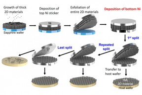 |
| Schematic illustration explaining the atomic scale manipulation of 2-D materials, in which thick wafer-scale 2-D materials are split into individual monolayers. Courtesy of the researchers |
Abstract:
Since the 2003 discovery of the single-atom-thick carbon material known as graphene, there has been significant interest in other types of 2-D materials as well.
Researchers quickly harvest 2-D materials, bringing them closer to commercialization: Efficient method for making single-atom-thick, wafer-scale materials opens up opportunities in flexible electronics
Cambridge, MA | Posted on October 12th, 2018These materials could be stacked together like Lego bricks to form a range of devices with different functions, including operating as semiconductors. In this way, they could be used to create ultra-thin, flexible, transparent and wearable electronic devices.
However, separating a bulk crystal material into 2-D flakes for use in electronics has proven difficult to do on a commercial scale.
The existing process, in which individual flakes are split off from the bulk crystals by repeatedly stamping the crystals onto an adhesive tape, is unreliable and time-consuming, requiring many hours to harvest enough material and form a device.
Now researchers in the Department of Mechanical Engineering at MIT have developed a technique to harvest 2-inch diameter wafers of 2-D material within just a few minutes. They can then be stacked together to form an electronic device within an hour.
The technique, which they describe in a paper published in the journal Science, could open up the possibility of commercializing electronic devices based on a variety of 2-D materials, according to Jeehwan Kim, an associate professor in the Department of Mechanical Engineering, who led the research.
The paper's co-first authors were Sanghoon Bae, who was involved in flexible device fabrication, and Jaewoo Shim, who worked on the stacking of the 2-D material monolayers. Both are postdocs in Kim's group.
The paper's co-authors also included students and postdocs from within Kim's group, as well as collaborators at Georgia Tech, the University of Texas, Yonsei University in South Korea, and the University of Virginia. Sang-Hoon Bae, Jaewoo Shim, Wei Kong, and Doyoon Lee in Kim's research group equally contributed to this work.
"We have shown that we can do monolayer-by-monolayer isolation of 2-D materials at the wafer scale," Kim says. "Secondly, we have demonstrated a way to easily stack up these wafer-scale monolayers of 2-D material."
The researchers first grew a thick stack of 2-D material on top of a sapphire wafer. They then applied a 600-nanometer-thick nickel film to the top of the stack.
Since 2-D materials adhere much more strongly to nickel than to sapphire, lifting off this film allowed the researchers to separate the entire stack from the wafer.
What's more, the adhesion between the nickel and the individual layers of 2-D material is also greater than that between each of the layers themselves.
As a result, when a second nickel film was then added to the bottom of the stack, the researchers were able to peel off individual, single-atom thick monolayers of 2-D material.
That is because peeling off the first nickel film generates cracks in the material that propagate right through to the bottom of the stack, Kim says.
Once the first monolayer collected by the nickel film has been transferred to a substrate, the process can be repeated for each layer.
"We use very simple mechanics, and by using this controlled crack propagation concept we are able to isolate monolayer 2-D material at the wafer scale," he says.
The universal technique can be used with a range of different 2-D materials, including hexagonal boron nitride, tungsten disulfide, and molybdenum disulfide.
In this way it can be used to produce different types of monolayer 2-D materials, such as semiconductors, metals, and insulators, which can then be stacked together to form the 2-D heterostructures needed for an electronic device.
"If you fabricate electronic and photonic devices using 2-D materials, the devices will be just a few monolayers thick," Kim says. "They will be extremely flexible, and can be stamped on to anything," he says.
The process is fast and low-cost, making it suitable for commercial operations, he adds.
The researchers have also demonstrated the technique by successfully fabricating arrays of field-effect transistors at the wafer scale, with a thickness of just a few atoms.
"The work has a lot of potential to bring 2-D materials and their heterostructures towards real-world applications," says Philip Kim, a professor of physics at Harvard University, who was not involved in the research.
The researchers are now planning to apply the technique to develop a range of electronic devices, including a nonvolatile memory array and flexible devices that can be worn on the skin.
They are also interested in applying the technique to develop devices for use in the "internet of things," Kim says.
"All you need to do is grow these thick 2-D materials, then isolate them in monolayers and stack them up. So it is extremely cheap -- much cheaper than the existing semiconductor process. This means it will bring laboratory-level 2-D materials into manufacturing for commercialization," Kim says.
"That makes it perfect for IoT networks, because if you were to use conventional semiconductors for the sensing systems it would be expensive."
####
For more information, please click here
Contacts:
Abby Abazorius
617-253-2709
Copyright © Massachusetts Institute of Technology
If you have a comment, please Contact us.Issuers of news releases, not 7th Wave, Inc. or Nanotechnology Now, are solely responsible for the accuracy of the content.
Bookmark:


| Related News Press |
News and information
![]() Simulating magnetization in a Heisenberg quantum spin chain April 5th, 2024
Simulating magnetization in a Heisenberg quantum spin chain April 5th, 2024
![]() NRL charters Navy�s quantum inertial navigation path to reduce drift April 5th, 2024
NRL charters Navy�s quantum inertial navigation path to reduce drift April 5th, 2024
![]() Discovery points path to flash-like memory for storing qubits: Rice find could hasten development of nonvolatile quantum memory April 5th, 2024
Discovery points path to flash-like memory for storing qubits: Rice find could hasten development of nonvolatile quantum memory April 5th, 2024
2 Dimensional Materials
![]() NRL discovers two-dimensional waveguides February 16th, 2024
NRL discovers two-dimensional waveguides February 16th, 2024
Graphene/ Graphite
![]() NRL discovers two-dimensional waveguides February 16th, 2024
NRL discovers two-dimensional waveguides February 16th, 2024
Flexible Electronics
![]() Tin selenide nanosheets enables to develop wearable tracking devices December 9th, 2022
Tin selenide nanosheets enables to develop wearable tracking devices December 9th, 2022
Internet-of-Things
![]() New nanowire sensors are the next step in the Internet of Things January 6th, 2023
New nanowire sensors are the next step in the Internet of Things January 6th, 2023
![]() New chip ramps up AI computing efficiency August 19th, 2022
New chip ramps up AI computing efficiency August 19th, 2022
![]() Lightening up the nanoscale long-wavelength optoelectronics May 13th, 2022
Lightening up the nanoscale long-wavelength optoelectronics May 13th, 2022
Possible Futures
![]() Discovery points path to flash-like memory for storing qubits: Rice find could hasten development of nonvolatile quantum memory April 5th, 2024
Discovery points path to flash-like memory for storing qubits: Rice find could hasten development of nonvolatile quantum memory April 5th, 2024
![]() With VECSELs towards the quantum internet Fraunhofer: IAF achieves record output power with VECSEL for quantum frequency converters April 5th, 2024
With VECSELs towards the quantum internet Fraunhofer: IAF achieves record output power with VECSEL for quantum frequency converters April 5th, 2024
Sensors
Discoveries
![]() Chemical reactions can scramble quantum information as well as black holes April 5th, 2024
Chemical reactions can scramble quantum information as well as black holes April 5th, 2024
![]() New micromaterial releases nanoparticles that selectively destroy cancer cells April 5th, 2024
New micromaterial releases nanoparticles that selectively destroy cancer cells April 5th, 2024
![]() Utilizing palladium for addressing contact issues of buried oxide thin film transistors April 5th, 2024
Utilizing palladium for addressing contact issues of buried oxide thin film transistors April 5th, 2024
Announcements
![]() NRL charters Navy�s quantum inertial navigation path to reduce drift April 5th, 2024
NRL charters Navy�s quantum inertial navigation path to reduce drift April 5th, 2024
![]() Discovery points path to flash-like memory for storing qubits: Rice find could hasten development of nonvolatile quantum memory April 5th, 2024
Discovery points path to flash-like memory for storing qubits: Rice find could hasten development of nonvolatile quantum memory April 5th, 2024
|
|
||
|
|
||
| The latest news from around the world, FREE | ||
|
|
||
|
|
||
| Premium Products | ||
|
|
||
|
Only the news you want to read!
Learn More |
||
|
|
||
|
Full-service, expert consulting
Learn More |
||
|
|
||