Home > Press > Researchers Succeed in Localizing Individual Atoms in Nanostructures Using First Cryo-Transfer LEAP Atom Probe
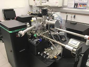 |
| CAMECA “Cyro-Transfer” LEAP Atom Probe |
Abstract:
Scientists from ETH Zürich and Oxford University have succeeded in mapping volatile hydrogen atoms in metal using the first "cryo-transfer" local electrode atom probe (LEAP®).
Researchers Succeed in Localizing Individual Atoms in Nanostructures Using First Cryo-Transfer LEAP Atom Probe
Madison, WI | Posted on April 19th, 2017The results of that milestone research project were published recently in Science (Direct observation of individual hydrogen atoms at trapping sites in a ferritic steel, Y.S. Chen et al. Science Vol. 355, pp 1196-1199 (17 Mar 2017), the peer-reviewed journal of the American Association for the Advancement of Science.
Hydrogen inclusions in metal can severely affect material properties, making the metal more brittle. To avoid failures in steel or other metals due to hydrogen embrittlement and cracks, scientists need to precisely locate the atoms of hydrogen.
Atom Probe Tomography (APT) has proven to be one of the best analytical techniques for identifying and determining the position of nearly every atom in three dimensions in almost any nanoscale material. Nevertheless, the 3-D mapping of hydrogen atoms has remained a challenge, even with improved APT instrumentation, because hydrogen atoms are so mobile.
Researchers at the University of Oxford, investigating the origins of hydrogen embrittlement, have teamed up with the materials research team at ETH Zürich, which has developed a unique cryogenic transfer protocol for its LEAP Atom Probe that allows researchers to immobilize the highly diffusive hydrogen in the microstructure before APT analysis.
Together, the researchers have succeeded in precisely identifying the mechanism by which a specific microstructure can trap individual hydrogen atoms within solid material using the ETH Zürich LEAP Atom Probe.
The ETH Zürich and Oxford University scientists are confident that their low-temperature APT protocol can be used for many other materials, including rubber or polymers, and even liquids!
About Atom Probe Tomography
Exclusively developed and manufactured by CAMECA®, atom probe microscopes are used by the most prestigious research and development laboratories around the world. Atom probe tomography (APT or 3D APT) is the only materials analysis technique that offers extensive capabilities for both 3-D imaging and chemical composition measurements at the atomic scale. The technique has contributed to a number of major advances in materials science since its development in the 1960s.
CAMECA’s Atom Probe Tomography product line comprises two families: the LEAP 5000 (Local Electrode Atom Probe) family, which provides the fastest, most sensitive 3-D imaging and analysis with nanoscale resolution across the widest range of applications (metals, oxides, ceramics, advanced energy storage materials, semiconductors and electronics, bio-minerals and geochemistry), and the newly launched EIKOS family, which offers accessibility to atom probe tomography with improved ease of use and a low cost of ownership for both general research and industrial applications.
####
About CAMECA
CAMECA has more than 60 years of experience in the design, manufacture and servicing of scientific instruments for material micro- and nano-analysis. Since pioneering Electron Probe Microanalysis (EPMA) instrumentation in the 1950s and Secondary Ion Mass Spectrometry (SIMS) in the 1960s, CAMECA has remained the undisputed world leader, while achieving numerous breakthrough innovations in such complementary techniques as Low-energy Electron-induced X-ray Emission Spectrometry (LEXES) and Atom Probe Tomography (APT).
With the acquisition and integration of Nu Instruments in 2016, CAMECA strengthened its product offering and technical capabilities in elemental and isotopic mass spectrometry with Inductively Coupled Plasma Mass Spectrometry (ICP-MS), Glow Discharge Mass Spectrometry (GD-MS) and Thermal Ionisation Mass Spectrometry (TIMS).
Headquartered near Paris, CAMECA has additional production facilities in Madison WI, USA, and Wrexham, UK, as well as sales, service and support locations in Brazil, China, Germany, India, Japan, Korea, Russia and Taiwan. CAMECA is a business unit of the Materials Analysis Division of AMETEK, Inc., a leading global manufacturer of electronic instruments and electromechanical products.
For more information, please click here
Contacts:
Marion Chopin
+33 1 433 46250
Copyright © CAMECA
If you have a comment, please Contact us.Issuers of news releases, not 7th Wave, Inc. or Nanotechnology Now, are solely responsible for the accuracy of the content.
Bookmark:


| Related News Press |
News and information
![]() Simulating magnetization in a Heisenberg quantum spin chain April 5th, 2024
Simulating magnetization in a Heisenberg quantum spin chain April 5th, 2024
![]() NRL charters Navy’s quantum inertial navigation path to reduce drift April 5th, 2024
NRL charters Navy’s quantum inertial navigation path to reduce drift April 5th, 2024
![]() Discovery points path to flash-like memory for storing qubits: Rice find could hasten development of nonvolatile quantum memory April 5th, 2024
Discovery points path to flash-like memory for storing qubits: Rice find could hasten development of nonvolatile quantum memory April 5th, 2024
Discoveries
![]() Chemical reactions can scramble quantum information as well as black holes April 5th, 2024
Chemical reactions can scramble quantum information as well as black holes April 5th, 2024
![]() New micromaterial releases nanoparticles that selectively destroy cancer cells April 5th, 2024
New micromaterial releases nanoparticles that selectively destroy cancer cells April 5th, 2024
![]() Utilizing palladium for addressing contact issues of buried oxide thin film transistors April 5th, 2024
Utilizing palladium for addressing contact issues of buried oxide thin film transistors April 5th, 2024
Announcements
![]() NRL charters Navy’s quantum inertial navigation path to reduce drift April 5th, 2024
NRL charters Navy’s quantum inertial navigation path to reduce drift April 5th, 2024
![]() Discovery points path to flash-like memory for storing qubits: Rice find could hasten development of nonvolatile quantum memory April 5th, 2024
Discovery points path to flash-like memory for storing qubits: Rice find could hasten development of nonvolatile quantum memory April 5th, 2024
Tools
![]() Ferroelectrically modulate the Fermi level of graphene oxide to enhance SERS response November 3rd, 2023
Ferroelectrically modulate the Fermi level of graphene oxide to enhance SERS response November 3rd, 2023
![]() The USTC realizes In situ electron paramagnetic resonance spectroscopy using single nanodiamond sensors November 3rd, 2023
The USTC realizes In situ electron paramagnetic resonance spectroscopy using single nanodiamond sensors November 3rd, 2023
|
|
||
|
|
||
| The latest news from around the world, FREE | ||
|
|
||
|
|
||
| Premium Products | ||
|
|
||
|
Only the news you want to read!
Learn More |
||
|
|
||
|
Full-service, expert consulting
Learn More |
||
|
|
||