Home > Press > Crystalline Fault Lines Provide Pathway for Solar Cell Current: New tomographic AFM imaging technique reveals that microstructural defects, generally thought to be detrimental, actually improve conductivity in cadmium telluride solar cells
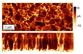 |
| These CTAFM images show a cadmium telluride solar cell from the top (above) and side profile (bottom) with bright spots representing areas of higher electron conductivity. The images reveal that the conductive pathways coincide with crystal grain boundaries. Credit: University of Connecticut. |
Abstract:
A team of scientists studying solar cells made from cadmium telluride, a promising alternative to silicon, has discovered that microscopic "fault lines" within and between crystals of the material act as conductive pathways that ease the flow of electric current. This research-conducted at the University of Connecticut and the U.S. Department of Energy's Brookhaven National Laboratory, and described in the journal Nature Energy-may help explain how a common processing technique turns cadmium telluride into an excellent material for transforming sunlight into electricity, and suggests a strategy for engineering more efficient solar devices that surpass the performance of silicon.
Crystalline Fault Lines Provide Pathway for Solar Cell Current: New tomographic AFM imaging technique reveals that microstructural defects, generally thought to be detrimental, actually improve conductivity in cadmium telluride solar cells
Upton, NY | Posted on September 26th, 2016"If you look at semiconductors like silicon, defects in the crystals are usually bad," said co-author Eric Stach, a physicist at Brookhaven Lab's Center for Functional Nanomaterials (CFN). As Stach explained, misplaced atoms or slight shifts in their alignment often act as traps for the particles that carry electric current-negatively charged electrons or the positively charged "holes" left behind when electrons are knocked loose by photons of sunlight, making them more mobile. The idea behind solar cells is to separate the positive and negative charges and run them through a circuit so the current can be used to power houses, satellites, or even cities. Defects interrupt this flow of charges and keep the solar cell from being as efficient as it could be.
But in the case of cadmium telluride, the scientists found that boundaries between individual crystals and "planar defects"-fault-like misalignments in the arrangement of atoms-create pathways for conductivity, not traps.
Members of Bryan Huey's group at the Institute of Materials Science at the University of Connecticut were the first to notice the surprising connection. In an effort to understand the effects of a chloride solution treatment that greatly enhances cadmium telluride's conductive properties, Justin Luria and Yasemin Kutes studied solar cells before and after treatment. But they did so in a unique way.
Several groups around the world had looked at the surfaces of such solar cells before, often with a tool known as a conducting atomic force microscope. The microscope has a fine probe many times sharper than the head of a pin that scans across the material's surface to track the topographic features-the hills and valleys of the surface structure-while simultaneously measuring location-specific conductivity. Scientists use this technique to explore how the surface features relate to solar cell performance at the nanoscale.
But no one had devised a way to make measurements beneath the surface, the most important part of the solar cell. This is where the UConn team made an important breakthrough. They used an approach developed and perfected by Kutes and Luria over the last two years to acquire hundreds of sequential images, each time intentionally removing a nanoscale layer of the material, so they could scan through the entire thickness of the sample. They then used these layer-by-layer images to build up a three-dimensional, high-resolution 'tomographic' map of the solar cell-somewhat like a computed tomography (CT) brain scan.
"Everyone using these microscopes basically takes pictures of the 'ground,' and interprets what is beneath," Huey said. "It may look like there's a cave, or a rock shelf, or a building foundation down there. But we can only really know once we carefully dig, like archeologists, keeping track of exactly what we find every step of the way-though, of course, at a much, much smaller scale."
The resulting CT-AFM maps uniquely revealed current flowing most freely along the crystal boundaries and fault-like defects in the cadmium telluride solar cells. The samples that had been treated with the chloride solution had more defects overall, a higher density of these defects, and what appeared to be a high degree of connectivity among them, while the untreated samples had few defects, no evidence of connectivity, and much lower conductivity.
Huey's team suspected that the defects were so-called planar defects, usually caused by shifts in atomic alignments or stacking arrangements within the crystals. But the CTAFM system is not designed to reveal such atomic-scale structural details. To get that information, the UConn team turned to Stach, head of the electron microscopy group at the CFN, a DOE Office of Science User Facility.
"Having previously shared ideas with Eric, it was a natural extension of our discovery to work with his group," Huey said.
Said Stach, "This is the exact type of problem the CFN is set up to handle, providing expertise and equipment that university researchers may not have to help drive science from hypothesis to discovery."
CFN staff physicist Lihua Zhang used a transmission electron microscope (TEM) and UConn's results as a guide to meticulously study how atomic scale features of chloride-treated cadmium telluride related to the conductivity maps. The TEM images revealed the atomic structure of the defects, confirming that they were due to specific changes in the stacking sequence of atoms in the material. The images also showed clearly that these planar defects connected different grains in the crystal, leading to high-conductivity pathways for the movement of electrons and holes.
"When we looked at the regions with good conductivity, the planar defects linked from one crystal grain to another, forming continuous pathways of conductance through the entire thickness of the material," said Zhang. "So the regions that had the best conductivity were the ones that had a high degree of connectivity among these defects."
The authors say it's possible that the chloride treatment helps to create the connectivity, not just more defects, but that more research is needed to definitively determine the most significant effects of the chloride solution treatment.
In any case, Stach says that combining the CTAFM technique and electron microscopy, yields a "clear winner" in the search for more efficient, cost-competitive alternatives to silicon solar cells, which have nearly reached their limit for efficiency.
"There is already a billion-dollar-a-year industry making cadmium telluride solar cells, and lots of work exploring other alternatives to silicon. But all of these alternatives, because of their crystal structure, have a higher tendency to form defects," he said. "This work gives us a systematic method we can use to understand if the defects are good or bad in terms of conductivity. It can also be used to explore the effects of different processing methods or chemicals to control how defects form. In the case of cadmium telluride, we may want to find ways to make more of these defects, or look for other materials in which defects improve performance."
This research was supported by the DOE Office of Energy Efficiency and Renewable Energy (EERE)-including its Sunshot Program-and the DOE Office of Science. The cadmium telluride samples were provided by Andrew Moore of Colorado State University.
The University of Connecticut's Institute of Materials Science serves as the heart of materials science research at the University of Connecticut, with a mission of supporting materials research and industry throughout Connecticut and the Northeast. It houses the research labs of more than 30 core faculty, with an overall membership of 120 UConn faculty whose work benefits from the available facilities and expertise.
####
About Brookhaven National Laboratory
Brookhaven National Laboratory is supported by the Office of Science of the U.S. Department of Energy. The Office of Science is the single largest supporter of basic research in the physical sciences in the United States, and is working to address some of the most pressing challenges of our time. For more information, please visit science.energy.gov.
One of ten national laboratories overseen and primarily funded by the Office of Science of the U.S. Department of Energy (DOE), Brookhaven National Laboratory conducts research in the physical, biomedical, and environmental sciences, as well as in energy technologies and national security. Brookhaven Lab also builds and operates major scientific facilities available to university, industry and government researchers. Brookhaven is operated and managed for DOE's Office of Science by Brookhaven Science Associates, a limited-liability company founded by the Research Foundation for the State University of New York on behalf of Stony Brook University, the largest academic user of Laboratory facilities, and Battelle, a nonprofit applied science and technology organization.
For more information, please click here
Contacts:
Karen McNulty Walsh
(631) 344-8350
or
Peter Genzer
(631) 344-3174
Copyright © Brookhaven National Laboratory
If you have a comment, please Contact us.Issuers of news releases, not 7th Wave, Inc. or Nanotechnology Now, are solely responsible for the accuracy of the content.
Bookmark:


| Related Links |
| Related News Press |
News and information
![]() Simulating magnetization in a Heisenberg quantum spin chain April 5th, 2024
Simulating magnetization in a Heisenberg quantum spin chain April 5th, 2024
![]() NRL charters Navy�s quantum inertial navigation path to reduce drift April 5th, 2024
NRL charters Navy�s quantum inertial navigation path to reduce drift April 5th, 2024
![]() Discovery points path to flash-like memory for storing qubits: Rice find could hasten development of nonvolatile quantum memory April 5th, 2024
Discovery points path to flash-like memory for storing qubits: Rice find could hasten development of nonvolatile quantum memory April 5th, 2024
Laboratories
![]() A battery�s hopping ions remember where they�ve been: Seen in atomic detail, the seemingly smooth flow of ions through a battery�s electrolyte is surprisingly complicated February 16th, 2024
A battery�s hopping ions remember where they�ve been: Seen in atomic detail, the seemingly smooth flow of ions through a battery�s electrolyte is surprisingly complicated February 16th, 2024
![]() NRL discovers two-dimensional waveguides February 16th, 2024
NRL discovers two-dimensional waveguides February 16th, 2024
![]() Three-pronged approach discerns qualities of quantum spin liquids November 17th, 2023
Three-pronged approach discerns qualities of quantum spin liquids November 17th, 2023
Govt.-Legislation/Regulation/Funding/Policy
![]() NRL charters Navy�s quantum inertial navigation path to reduce drift April 5th, 2024
NRL charters Navy�s quantum inertial navigation path to reduce drift April 5th, 2024
![]() Discovery points path to flash-like memory for storing qubits: Rice find could hasten development of nonvolatile quantum memory April 5th, 2024
Discovery points path to flash-like memory for storing qubits: Rice find could hasten development of nonvolatile quantum memory April 5th, 2024
![]() Chemical reactions can scramble quantum information as well as black holes April 5th, 2024
Chemical reactions can scramble quantum information as well as black holes April 5th, 2024
Possible Futures
![]() Discovery points path to flash-like memory for storing qubits: Rice find could hasten development of nonvolatile quantum memory April 5th, 2024
Discovery points path to flash-like memory for storing qubits: Rice find could hasten development of nonvolatile quantum memory April 5th, 2024
![]() With VECSELs towards the quantum internet Fraunhofer: IAF achieves record output power with VECSEL for quantum frequency converters April 5th, 2024
With VECSELs towards the quantum internet Fraunhofer: IAF achieves record output power with VECSEL for quantum frequency converters April 5th, 2024
Discoveries
![]() Chemical reactions can scramble quantum information as well as black holes April 5th, 2024
Chemical reactions can scramble quantum information as well as black holes April 5th, 2024
![]() New micromaterial releases nanoparticles that selectively destroy cancer cells April 5th, 2024
New micromaterial releases nanoparticles that selectively destroy cancer cells April 5th, 2024
![]() Utilizing palladium for addressing contact issues of buried oxide thin film transistors April 5th, 2024
Utilizing palladium for addressing contact issues of buried oxide thin film transistors April 5th, 2024
Materials/Metamaterials/Magnetoresistance
![]() Nanoscale CL thermometry with lanthanide-doped heavy-metal oxide in TEM March 8th, 2024
Nanoscale CL thermometry with lanthanide-doped heavy-metal oxide in TEM March 8th, 2024
![]() Focused ion beam technology: A single tool for a wide range of applications January 12th, 2024
Focused ion beam technology: A single tool for a wide range of applications January 12th, 2024
Announcements
![]() NRL charters Navy�s quantum inertial navigation path to reduce drift April 5th, 2024
NRL charters Navy�s quantum inertial navigation path to reduce drift April 5th, 2024
![]() Discovery points path to flash-like memory for storing qubits: Rice find could hasten development of nonvolatile quantum memory April 5th, 2024
Discovery points path to flash-like memory for storing qubits: Rice find could hasten development of nonvolatile quantum memory April 5th, 2024
Interviews/Book Reviews/Essays/Reports/Podcasts/Journals/White papers/Posters
![]() Simulating magnetization in a Heisenberg quantum spin chain April 5th, 2024
Simulating magnetization in a Heisenberg quantum spin chain April 5th, 2024
![]() Discovery points path to flash-like memory for storing qubits: Rice find could hasten development of nonvolatile quantum memory April 5th, 2024
Discovery points path to flash-like memory for storing qubits: Rice find could hasten development of nonvolatile quantum memory April 5th, 2024
Energy
![]() Development of zinc oxide nanopagoda array photoelectrode: photoelectrochemical water-splitting hydrogen production January 12th, 2024
Development of zinc oxide nanopagoda array photoelectrode: photoelectrochemical water-splitting hydrogen production January 12th, 2024
![]() Shedding light on unique conduction mechanisms in a new type of perovskite oxide November 17th, 2023
Shedding light on unique conduction mechanisms in a new type of perovskite oxide November 17th, 2023
![]() Inverted perovskite solar cell breaks 25% efficiency record: Researchers improve cell efficiency using a combination of molecules to address different November 17th, 2023
Inverted perovskite solar cell breaks 25% efficiency record: Researchers improve cell efficiency using a combination of molecules to address different November 17th, 2023
![]() The efficient perovskite cells with a structured anti-reflective layer � another step towards commercialization on a wider scale October 6th, 2023
The efficient perovskite cells with a structured anti-reflective layer � another step towards commercialization on a wider scale October 6th, 2023
Research partnerships
![]() Discovery points path to flash-like memory for storing qubits: Rice find could hasten development of nonvolatile quantum memory April 5th, 2024
Discovery points path to flash-like memory for storing qubits: Rice find could hasten development of nonvolatile quantum memory April 5th, 2024
![]() Researchers� approach may protect quantum computers from attacks March 8th, 2024
Researchers� approach may protect quantum computers from attacks March 8th, 2024
![]() 'Sudden death' of quantum fluctuations defies current theories of superconductivity: Study challenges the conventional wisdom of superconducting quantum transitions January 12th, 2024
'Sudden death' of quantum fluctuations defies current theories of superconductivity: Study challenges the conventional wisdom of superconducting quantum transitions January 12th, 2024
Solar/Photovoltaic
![]() Development of zinc oxide nanopagoda array photoelectrode: photoelectrochemical water-splitting hydrogen production January 12th, 2024
Development of zinc oxide nanopagoda array photoelectrode: photoelectrochemical water-splitting hydrogen production January 12th, 2024
![]() Shedding light on unique conduction mechanisms in a new type of perovskite oxide November 17th, 2023
Shedding light on unique conduction mechanisms in a new type of perovskite oxide November 17th, 2023
![]() Inverted perovskite solar cell breaks 25% efficiency record: Researchers improve cell efficiency using a combination of molecules to address different November 17th, 2023
Inverted perovskite solar cell breaks 25% efficiency record: Researchers improve cell efficiency using a combination of molecules to address different November 17th, 2023
![]() Charged �molecular beasts� the basis for new compounds: Researchers at Leipzig University use �aggressive� fragments of molecular ions for chemical synthesis November 3rd, 2023
Charged �molecular beasts� the basis for new compounds: Researchers at Leipzig University use �aggressive� fragments of molecular ions for chemical synthesis November 3rd, 2023
|
|
||
|
|
||
| The latest news from around the world, FREE | ||
|
|
||
|
|
||
| Premium Products | ||
|
|
||
|
Only the news you want to read!
Learn More |
||
|
|
||
|
Full-service, expert consulting
Learn More |
||
|
|
||