Home > Press > Engineering material magic: Utah engineers discover groundbreaking semiconducting material that could lead to much faster electronics
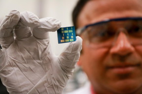 |
| University of Utah materials science and engineering associate professor Ashutosh Tiwari holds up a substrate layered with a newly discovered 2-D material made of tin and oxygen. Tiwari and his team have discovered this new material, tin monoxide, which allows electrical charges to move through it much faster than common 3-D material such as silicon. This breakthrough in semiconductor material could lead to much faster computers and mobile devices such as smartphones that also run on less power and with less heat. CREDIT: Dan Hixson/University of Utah College of Engineering |
Abstract:
University of Utah engineers have discovered a new kind of 2D semiconducting material for electronics that opens the door for much speedier computers and smartphones that also consume a lot less power.
Engineering material magic: Utah engineers discover groundbreaking semiconducting material that could lead to much faster electronics
Salt Lake City, UT | Posted on February 15th, 2016The semiconductor, made of the elements tin and oxygen, or tin monoxide (SnO), is a layer of 2D material only one atom thick, allowing electrical charges to move through it much faster than conventional 3D materials such as silicon. This material could be used in transistors, the lifeblood of all electronic devices such as computer processors and graphics processors in desktop computers and mobile devices. The material was discovered by a team led by University of Utah materials science and engineering associate professor Ashutosh Tiwari. A paper describing the research was published online Monday, Feb. 15, 2016 in the journal, Advanced Electronic Materials. The paper, which also will be the cover story on the printed version of the journal, was co-authored by University of Utah materials science and engineering doctoral students K. J. Saji and Kun Tian, and Michael Snure of the Wright-Patterson Air Force Research Lab near Dayton, Ohio.
Transistors and other components used in electronic devices are currently made of 3D materials such as silicon and consist of multiple layers on a glass substrate. But the downside to 3D materials is that electrons bounce around inside the layers in all directions.
The benefit of 2D materials, which is an exciting new research field that has opened up only about five years ago, is that the material is made of one layer the thickness of just one or two atoms. Consequently, the electrons "can only move in one layer so it's much faster," says Tiwari.
While researchers in this field have recently discovered new types of 2D material such as graphene, molybdenun disulfide and borophene, they have been materials that only allow the movement of N-type, or negative, electrons. In order to create an electronic device, however, you need semiconductor material that allows the movement of both negative electrons and positive charges known as "holes." The tin monoxide material discovered by Tiwari and his team is the first stable P-type 2D semiconductor material ever in existence.
"Now we have everything -- we have P-type 2D semiconductors and N-type 2D semiconductors," he says. "Now things will move forward much more quickly."
Now that Tiwari and his team have discovered this new 2D material, it can lead to the manufacturing of transistors that are even smaller and faster than those in use today. A computer processor is comprised of billions of transistors, and the more transistors packed into a single chip, the more powerful the processor can become.
Transistors made with Tiwari's semiconducting material could lead to computers and smartphones that are more than 100 times faster than regular devices. And because the electrons move through one layer instead of bouncing around in a 3D material, there will be less friction, meaning the processors will not get as hot as normal computer chips. They also will require much less power to run, a boon for mobile electronics that have to run on battery power. Tiwari says this could be especially important for medical devices such as electronic implants that will run longer on a single battery charge.
"The field is very hot right now, and people are very interested in it," Tiwari says. "So in two or three years we should see at least some prototype device."
####
For more information, please click here
Contacts:
Vincent Horiuchi
801-585-7499
Copyright © University of Utah
If you have a comment, please Contact us.Issuers of news releases, not 7th Wave, Inc. or Nanotechnology Now, are solely responsible for the accuracy of the content.
Bookmark:


| Related News Press |
News and information
![]() Researchers develop molecular qubits that communicate at telecom frequencies October 3rd, 2025
Researchers develop molecular qubits that communicate at telecom frequencies October 3rd, 2025
![]() Next-generation quantum communication October 3rd, 2025
Next-generation quantum communication October 3rd, 2025
![]() "Nanoreactor" cage uses visible light for catalytic and ultra-selective cross-cycloadditions October 3rd, 2025
"Nanoreactor" cage uses visible light for catalytic and ultra-selective cross-cycloadditions October 3rd, 2025
Friction/ Tribology
![]() Perking up and crimping the 'bristles' of polyelectrolyte brushes December 13th, 2017
Perking up and crimping the 'bristles' of polyelectrolyte brushes December 13th, 2017
Possible Futures
![]() Spinel-type sulfide semiconductors to operate the next-generation LEDs and solar cells For solar-cell absorbers and green-LED source October 3rd, 2025
Spinel-type sulfide semiconductors to operate the next-generation LEDs and solar cells For solar-cell absorbers and green-LED source October 3rd, 2025
Chip Technology
![]() Lab to industry: InSe wafer-scale breakthrough for future electronics August 8th, 2025
Lab to industry: InSe wafer-scale breakthrough for future electronics August 8th, 2025
![]() A 1960s idea inspires NBI researchers to study hitherto inaccessible quantum states June 6th, 2025
A 1960s idea inspires NBI researchers to study hitherto inaccessible quantum states June 6th, 2025
![]() Programmable electron-induced color router array May 14th, 2025
Programmable electron-induced color router array May 14th, 2025
Nanoelectronics
![]() Lab to industry: InSe wafer-scale breakthrough for future electronics August 8th, 2025
Lab to industry: InSe wafer-scale breakthrough for future electronics August 8th, 2025
![]() Interdisciplinary: Rice team tackles the future of semiconductors Multiferroics could be the key to ultralow-energy computing October 6th, 2023
Interdisciplinary: Rice team tackles the future of semiconductors Multiferroics could be the key to ultralow-energy computing October 6th, 2023
![]() Key element for a scalable quantum computer: Physicists from Forschungszentrum J�lich and RWTH Aachen University demonstrate electron transport on a quantum chip September 23rd, 2022
Key element for a scalable quantum computer: Physicists from Forschungszentrum J�lich and RWTH Aachen University demonstrate electron transport on a quantum chip September 23rd, 2022
![]() Reduced power consumption in semiconductor devices September 23rd, 2022
Reduced power consumption in semiconductor devices September 23rd, 2022
Discoveries
![]() Researchers develop molecular qubits that communicate at telecom frequencies October 3rd, 2025
Researchers develop molecular qubits that communicate at telecom frequencies October 3rd, 2025
![]() Next-generation quantum communication October 3rd, 2025
Next-generation quantum communication October 3rd, 2025
![]() "Nanoreactor" cage uses visible light for catalytic and ultra-selective cross-cycloadditions October 3rd, 2025
"Nanoreactor" cage uses visible light for catalytic and ultra-selective cross-cycloadditions October 3rd, 2025
Materials/Metamaterials/Magnetoresistance
![]() First real-time observation of two-dimensional melting process: Researchers at Mainz University unveil new insights into magnetic vortex structures August 8th, 2025
First real-time observation of two-dimensional melting process: Researchers at Mainz University unveil new insights into magnetic vortex structures August 8th, 2025
![]() Researchers unveil a groundbreaking clay-based solution to capture carbon dioxide and combat climate change June 6th, 2025
Researchers unveil a groundbreaking clay-based solution to capture carbon dioxide and combat climate change June 6th, 2025
![]() A 1960s idea inspires NBI researchers to study hitherto inaccessible quantum states June 6th, 2025
A 1960s idea inspires NBI researchers to study hitherto inaccessible quantum states June 6th, 2025
![]() Institute for Nanoscience hosts annual proposal planning meeting May 16th, 2025
Institute for Nanoscience hosts annual proposal planning meeting May 16th, 2025
Announcements
![]() Rice membrane extracts lithium from brines with greater speed, less waste October 3rd, 2025
Rice membrane extracts lithium from brines with greater speed, less waste October 3rd, 2025
![]() Researchers develop molecular qubits that communicate at telecom frequencies October 3rd, 2025
Researchers develop molecular qubits that communicate at telecom frequencies October 3rd, 2025
![]() Next-generation quantum communication October 3rd, 2025
Next-generation quantum communication October 3rd, 2025
![]() "Nanoreactor" cage uses visible light for catalytic and ultra-selective cross-cycloadditions October 3rd, 2025
"Nanoreactor" cage uses visible light for catalytic and ultra-selective cross-cycloadditions October 3rd, 2025
Interviews/Book Reviews/Essays/Reports/Podcasts/Journals/White papers/Posters
![]() Spinel-type sulfide semiconductors to operate the next-generation LEDs and solar cells For solar-cell absorbers and green-LED source October 3rd, 2025
Spinel-type sulfide semiconductors to operate the next-generation LEDs and solar cells For solar-cell absorbers and green-LED source October 3rd, 2025
![]() Rice membrane extracts lithium from brines with greater speed, less waste October 3rd, 2025
Rice membrane extracts lithium from brines with greater speed, less waste October 3rd, 2025
|
|
||
|
|
||
| The latest news from around the world, FREE | ||
|
|
||
|
|
||
| Premium Products | ||
|
|
||
|
Only the news you want to read!
Learn More |
||
|
|
||
|
Full-service, expert consulting
Learn More |
||
|
|
||