Home > Press > Novel 'crumpling' of hybrid nanostructures increases SERS sensitivity
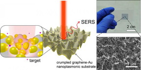 |
| Illustration of SERS enhancement from a crumpled graphene-Au nanoparticles hybrid structure. Raman spectrum is enhanced the most when the target molecule is situated at the center of Au nanoparticles in valley of crumpled graphene as depicted in inset. CREDIT: University of Illinois |
Abstract:
By "crumpling" to increase the surface area of graphene-gold nanostructures, researchers from the University of Illinois at Urbana-Champaign have improved the sensitivity of these materials, opening the door to novel opportunities in electronics and optical sensing applications.
Novel 'crumpling' of hybrid nanostructures increases SERS sensitivity
Urbana, IL | Posted on November 4th, 2015"I believe that this work will benefit researchers in the area of surface plasmonics by providing a new strategy/design for enhancing the surface enhanced Raman spectroscopy (SERS) detection limit," explained SungWoo Nam, an assistant professor of mechanical science and engineering at Illinois. "This mechanical self-assembly strategy will enable a new class of 3D crumpled graphene?gold (Au) nanostructures. The enhanced limit of detection will allow biomedical and environment monitoring of important molecules at high sensitivity by SERS."
SERS substrates are used to analyze the composition of a mixture at the nanoscale for environmental analysis, pharmaceuticals, material sciences, art and archeological research, forensic science, drug detection, food quality analysis, and single cell detection. Using a combination of gold and silver nanoparticles and Raman-active dyes, SERS substrates also can target specific DNA and RNA sequences.
"This work demonstrates the unique capability of micro-to-nanoscale topographies of the crumpled graphene-Au nanoparticles--higher density, three-dimensional optically active materials--that are further enhanced by the formation of hot spots, bringing the nanoparticles closer," explained Juyoung Leem, a graduate student and first author of the study, "Mechanically Self-Assembled, Three-Dimensional Graphene?Gold Hybrid Nanostructures for Advanced Nanoplasmonic Sensors," published in Nano Letters. "We achieve a 3D crumpled graphene?Au hybrid structure by the delamination and buckling of graphene on a thermally activated, shrinking polymer substrate. This process enables precise control and optimization of the size and spacing of integrated Au nanoparticles on crumpled graphene for higher SERS enhancement."
According to Nam, the 3D crumpled graphene?Au nanostructure exhibits at least one order of magnitude higher SERS detection sensitivity than that of conventional, flat graphene?Au nanoparticles. The hybrid structure is further adapted to arbitrary curvilinear structures for advanced, in situ, nonconventional, nanoplasmonic sensing applications.
"One of the key advantages of our platform is its ability to shrink and adapt to complex 3D surfaces, a function that has not been previously demonstrated," Nam stated. An earlier study by Nam's research group was the first to demonstrate graphene integration onto a variety of different microstructured geometries, including pyramids, pillars, domes, inverted pyramids, and the 3D integration of gold nanoparticle/graphene hybrid structures.
###
In addition to Leem and Nam, the study's co-authors include post-doctoral researcher Pilgyu Kang and graduate student Michael Cai Wang in the Department of Mechanical Sciences and Engineering. Experiments were carried out in part in the Frederick Seitz Materials Research Laboratory, the Micro and Nano Technology Laboratory, and the Beckman Institute Imaging Technology Group at Illinois.
####
For more information, please click here
Contacts:
SungWoo Nam
217-300-0267
Copyright © University of Illinois
If you have a comment, please Contact us.Issuers of news releases, not 7th Wave, Inc. or Nanotechnology Now, are solely responsible for the accuracy of the content.
Bookmark:


| Related News Press |
News and information
![]() Quantum computer improves AI predictions April 17th, 2026
Quantum computer improves AI predictions April 17th, 2026
![]() Flexible sensor gains sensitivity under pressure April 17th, 2026
Flexible sensor gains sensitivity under pressure April 17th, 2026
![]() A reusable chip for particulate matter sensing April 17th, 2026
A reusable chip for particulate matter sensing April 17th, 2026
![]() Detecting vibrational quantum beating in the predissociation dynamics of SF6 using time-resolved photoelectron spectroscopy April 17th, 2026
Detecting vibrational quantum beating in the predissociation dynamics of SF6 using time-resolved photoelectron spectroscopy April 17th, 2026
Graphene/ Graphite
![]() Electrifying results shed light on graphene foam as a potential material for lab grown cartilage June 6th, 2025
Electrifying results shed light on graphene foam as a potential material for lab grown cartilage June 6th, 2025
![]() Breakthrough in proton barrier films using pore-free graphene oxide: Kumamoto University researchers achieve new milestone in advanced coating technologies September 13th, 2024
Breakthrough in proton barrier films using pore-free graphene oxide: Kumamoto University researchers achieve new milestone in advanced coating technologies September 13th, 2024
Govt.-Legislation/Regulation/Funding/Policy
![]() Quantum computer improves AI predictions April 17th, 2026
Quantum computer improves AI predictions April 17th, 2026
![]() Metasurfaces smooth light to boost magnetic sensing precision January 30th, 2026
Metasurfaces smooth light to boost magnetic sensing precision January 30th, 2026
![]() New imaging approach transforms study of bacterial biofilms August 8th, 2025
New imaging approach transforms study of bacterial biofilms August 8th, 2025
Chip Technology
![]() A reusable chip for particulate matter sensing April 17th, 2026
A reusable chip for particulate matter sensing April 17th, 2026
![]() Metasurfaces smooth light to boost magnetic sensing precision January 30th, 2026
Metasurfaces smooth light to boost magnetic sensing precision January 30th, 2026
Optical computing/Photonic computing
![]() ICFO researchers overcome long-standing bottleneck in single photon detection with twisted 2D materials August 8th, 2025
ICFO researchers overcome long-standing bottleneck in single photon detection with twisted 2D materials August 8th, 2025
![]() Programmable electron-induced color router array May 14th, 2025
Programmable electron-induced color router array May 14th, 2025
Sensors
![]() Flexible sensor gains sensitivity under pressure April 17th, 2026
Flexible sensor gains sensitivity under pressure April 17th, 2026
![]() Tiny nanosheets, big leap: A new sensor detects ethanol at ultra-low levels January 30th, 2026
Tiny nanosheets, big leap: A new sensor detects ethanol at ultra-low levels January 30th, 2026
![]() From sensors to smart systems: the rise of AI-driven photonic noses January 30th, 2026
From sensors to smart systems: the rise of AI-driven photonic noses January 30th, 2026
![]() Sensors innovations for smart lithium-based batteries: advancements, opportunities, and potential challenges August 8th, 2025
Sensors innovations for smart lithium-based batteries: advancements, opportunities, and potential challenges August 8th, 2025
Discoveries
![]() Quantum computer improves AI predictions April 17th, 2026
Quantum computer improves AI predictions April 17th, 2026
![]() Flexible sensor gains sensitivity under pressure April 17th, 2026
Flexible sensor gains sensitivity under pressure April 17th, 2026
![]() A reusable chip for particulate matter sensing April 17th, 2026
A reusable chip for particulate matter sensing April 17th, 2026
![]() Detecting vibrational quantum beating in the predissociation dynamics of SF6 using time-resolved photoelectron spectroscopy April 17th, 2026
Detecting vibrational quantum beating in the predissociation dynamics of SF6 using time-resolved photoelectron spectroscopy April 17th, 2026
Materials/Metamaterials/Magnetoresistance
![]() First real-time observation of two-dimensional melting process: Researchers at Mainz University unveil new insights into magnetic vortex structures August 8th, 2025
First real-time observation of two-dimensional melting process: Researchers at Mainz University unveil new insights into magnetic vortex structures August 8th, 2025
![]() Researchers unveil a groundbreaking clay-based solution to capture carbon dioxide and combat climate change June 6th, 2025
Researchers unveil a groundbreaking clay-based solution to capture carbon dioxide and combat climate change June 6th, 2025
![]() A 1960s idea inspires NBI researchers to study hitherto inaccessible quantum states June 6th, 2025
A 1960s idea inspires NBI researchers to study hitherto inaccessible quantum states June 6th, 2025
![]() Institute for Nanoscience hosts annual proposal planning meeting May 16th, 2025
Institute for Nanoscience hosts annual proposal planning meeting May 16th, 2025
Announcements
![]() A fundamentally new therapeutic approach to cystic fibrosis: Nanobody repairs cellular defect April 17th, 2026
A fundamentally new therapeutic approach to cystic fibrosis: Nanobody repairs cellular defect April 17th, 2026
![]() UC Irvine physicists discover method to reverse �quantum scrambling� : The work addresses the problem of information loss in quantum computing system April 17th, 2026
UC Irvine physicists discover method to reverse �quantum scrambling� : The work addresses the problem of information loss in quantum computing system April 17th, 2026
Interviews/Book Reviews/Essays/Reports/Podcasts/Journals/White papers/Posters
![]() A fundamentally new therapeutic approach to cystic fibrosis: Nanobody repairs cellular defect April 17th, 2026
A fundamentally new therapeutic approach to cystic fibrosis: Nanobody repairs cellular defect April 17th, 2026
![]() UC Irvine physicists discover method to reverse �quantum scrambling� : The work addresses the problem of information loss in quantum computing system April 17th, 2026
UC Irvine physicists discover method to reverse �quantum scrambling� : The work addresses the problem of information loss in quantum computing system April 17th, 2026
Military
![]() Quantum engineers �squeeze� laser frequency combs to make more sensitive gas sensors January 17th, 2025
Quantum engineers �squeeze� laser frequency combs to make more sensitive gas sensors January 17th, 2025
![]() Chainmail-like material could be the future of armor: First 2D mechanically interlocked polymer exhibits exceptional flexibility and strength January 17th, 2025
Chainmail-like material could be the future of armor: First 2D mechanically interlocked polymer exhibits exceptional flexibility and strength January 17th, 2025
![]() Single atoms show their true color July 5th, 2024
Single atoms show their true color July 5th, 2024
![]() NRL charters Navy�s quantum inertial navigation path to reduce drift April 5th, 2024
NRL charters Navy�s quantum inertial navigation path to reduce drift April 5th, 2024
Photonics/Optics/Lasers
![]() Metasurfaces smooth light to boost magnetic sensing precision January 30th, 2026
Metasurfaces smooth light to boost magnetic sensing precision January 30th, 2026
![]() From sensors to smart systems: the rise of AI-driven photonic noses January 30th, 2026
From sensors to smart systems: the rise of AI-driven photonic noses January 30th, 2026
|
|
||
|
|
||
| The latest news from around the world, FREE | ||
|
|
||
|
|
||
| Premium Products | ||
|
|
||
|
Only the news you want to read!
Learn More |
||
|
|
||
|
Full-service, expert consulting
Learn More |
||
|
|
||