Home > Press > Eulitha unveils new photolithography system “Phabler 100” for photonic patterning
 |
Abstract:
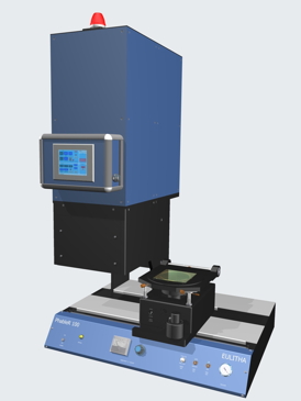
Eulitha AG, A Swiss based company specializing in novel nano lithography technologies, today announced the availability of a new photo-lithography system PhableR 100 for printing high resolution nano-structures, especially for research and development applications as well as pilot and low-volume production use. The system particularly targets the production of periodic patterns such as gratings and photonic crystals required in optics and photonics.
Eulitha unveils new photolithography system “Phabler 100” for photonic patterning
Villigen, Switzerland | Posted on December 12th, 2013The PhablerR 100 system is based on the proprietary PHABLE (short for Photonics Enabler) photolithographic technology developed by Eulitha AG, which makes it possible to print high-resolution structures in a non-contact, proximity photolithography system. The resolution obtained with the "PhableR 100" is essentially the same as what is obtainable from a DUV projection lithography system, but without the complex and expensive optics and mechanics of such a system. For example, linear gratings with a half-pitch of 150nm can be printed with high uniformity with the new system. As an added advantage, the practically unlimited depth of focus of the image formed by the PhableR 100 system means that the high-resolution patterns can be printed with high uniformity even onto non-flat substrates, which are commonly encountered in photonics applications.
The PhableR 100 system can expose substrates with diameters up to 100mm using industry standard chrome-on-glass or phase-shifting masks. The mask and the substrate are loaded manually onto the system and the exposure process is controlled by an onboard computer. Standard i-line photoresists, both positive and negative tone, which are available from common vendors, can be used. Linear or curved gratings, 2D photonic-crystal type patterns with hexagonal or square symmetry can be printed with feature periods less than 300nm. The system may also be used like a standard mask-aligner in either proximity or contact mode to print micron-scale structures. Targeted applications include research and development projects in photonics, fabrication of gratings for optical diffraction and spectroscopy, light extraction patterns on LEDs, patterned sapphire substrates and color filters.
Harun Solak, CEO of Eulitha AG stated "we are proud to introduce a solution that will enable our customers to perform high resolution photolithography with a low-cost system for the first time. This equipment is a result of a long-term development effort at both the Paul Scherrer Institut and Eulitha." The system is available for immediate demonstration at the Eulitha site in Switzerland. The PhableR 100 system will be presented at the 13th International Nanotechnology Exhibition which will take place between, January 29-21, 2013 in Tokyo, Japan.
####
About Eulitha AG
Eulitha AG is a spin-off company of the Paul Scherrer Institute, Switzerland. It specializes in the development of lithographic technologies for applications in photonics, biotech. It produces and markets nano-patterned samples and templates using its own PHABLE tools and state-of-the-art e-beam lithography systems. PHABLE is the brand name of its proprietary photolithography platform, which includes exposure tools and wafer patterning services.
For more information, please click here
Contacts:
Harun H. Solak
CEO
Tel: +41 56 310 4279
Rene Wilde
Sales Director
Tel: +41 56 281 2154
Copyright © Eulitha AG
If you have a comment, please Contact us.Issuers of news releases, not 7th Wave, Inc. or Nanotechnology Now, are solely responsible for the accuracy of the content.
Bookmark:


| Related News Press |
News and information
![]() Simulating magnetization in a Heisenberg quantum spin chain April 5th, 2024
Simulating magnetization in a Heisenberg quantum spin chain April 5th, 2024
![]() NRL charters Navy’s quantum inertial navigation path to reduce drift April 5th, 2024
NRL charters Navy’s quantum inertial navigation path to reduce drift April 5th, 2024
![]() Discovery points path to flash-like memory for storing qubits: Rice find could hasten development of nonvolatile quantum memory April 5th, 2024
Discovery points path to flash-like memory for storing qubits: Rice find could hasten development of nonvolatile quantum memory April 5th, 2024
Announcements
![]() NRL charters Navy’s quantum inertial navigation path to reduce drift April 5th, 2024
NRL charters Navy’s quantum inertial navigation path to reduce drift April 5th, 2024
![]() Discovery points path to flash-like memory for storing qubits: Rice find could hasten development of nonvolatile quantum memory April 5th, 2024
Discovery points path to flash-like memory for storing qubits: Rice find could hasten development of nonvolatile quantum memory April 5th, 2024
Tools
![]() Ferroelectrically modulate the Fermi level of graphene oxide to enhance SERS response November 3rd, 2023
Ferroelectrically modulate the Fermi level of graphene oxide to enhance SERS response November 3rd, 2023
![]() The USTC realizes In situ electron paramagnetic resonance spectroscopy using single nanodiamond sensors November 3rd, 2023
The USTC realizes In situ electron paramagnetic resonance spectroscopy using single nanodiamond sensors November 3rd, 2023
Events/Classes
![]() Researchers demonstrate co-propagation of quantum and classical signals: Study shows that quantum encryption can be implemented in existing fiber networks January 20th, 2023
Researchers demonstrate co-propagation of quantum and classical signals: Study shows that quantum encryption can be implemented in existing fiber networks January 20th, 2023
Printing/Lithography/Inkjet/Inks/Bio-printing/Dyes
![]() Presenting: Ultrasound-based printing of 3D materials—potentially inside the body December 8th, 2023
Presenting: Ultrasound-based printing of 3D materials—potentially inside the body December 8th, 2023
![]() Simple ballpoint pen can write custom LEDs August 11th, 2023
Simple ballpoint pen can write custom LEDs August 11th, 2023
![]() Disposable electronics on a simple sheet of paper October 7th, 2022
Disposable electronics on a simple sheet of paper October 7th, 2022
|
|
||
|
|
||
| The latest news from around the world, FREE | ||
|
|
||
|
|
||
| Premium Products | ||
|
|
||
|
Only the news you want to read!
Learn More |
||
|
|
||
|
Full-service, expert consulting
Learn More |
||
|
|
||