Home > Press > Invention jet prints nanostructures with self-assembling material
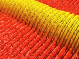 |
| This atomic force microscope image shows directed self-assembly of a printed line of block copolymer on a template prepared by photolithography. The microscope�s software colored and scaled the image. The density of patterns in the template (bounded by the thin lines) is two times that of the self-assembled structures (the ribbons). Courtesy of Serdar Onses/University of Illinois-Urbana |
Abstract:
A multi-institutional team of engineers has developed a new approach to the fabrication of nanostructures for the semiconductor and magnetic storage industries. This approach combines top-down advanced ink-jet printing technology with a bottom-up approach that involves self-assembling block copolymers, a type of material that can spontaneously form ultrafine structures.
Invention jet prints nanostructures with self-assembling material
Chicago, IL | Posted on September 16th, 2013The team, consisting of nine researchers from the University of Illinois at Urbana-Champaign, the University of Chicago and Hanyang University in Korea, was able to increase the resolution of their intricate structure fabrication from approximately 200 nanometers to approximately 15 nanometers. A nanometer is a billionth of a meter, the width of a double-stranded DNA molecule.
The ability to fabricate nanostructures out of polymers, DNA, proteins and other "soft" materials has the potential to enable new classes of electronics, diagnostic devices and chemical sensors. The challenge is that many of these materials are fundamentally incompatible with the sorts of lithographic techniques that are traditionally used in the integrated circuit industry.
Recently developed ultrahigh resolution ink-jet printing techniques have some potential, with demonstrated resolution down to 100-200 nanometers, but there are significant challenges in achieving true nanoscale dimension. "Our work demonstrates that processes of polymer self-assembly can provide a way around this limitation," said John Rogers, the Swanlund Chair Professor in Materials Science and Engineering at Illinois.
Rogers and his associates report their findings in the September issue of Nature Nanotechnology. Combining jet printing with self-assembling block copolymers enabled the engineers to attain the much higher resolution, as suggested by lead author Serdar Onses, a postdoctoral scientist at Illinois. Onses earned his doctorate at the University of Wisconsin under Paul Nealey, now the Brady W. Dougan Professor in Molecular Engineering at UChicago and a co-author of the Nature Nanotechnology paper. "This concept turned out to be really useful," Rogers said.
Engineers use self-assembling materials to augment traditional photolithographic processes that generate patterns for many technological applications. They first create either a topographical or chemical pattern using traditional processes. For the Nature Nanotechnology paper, this was done at imec in Belgium, an independent nanoelectronics research center. Nealey's laboratory pioneered this process of directed self-assembly of block copolymers using chemical nanopatterns.
Nearing the limits
The resolution of the chemical pattern nears the current limit of traditional photolithography, noted Lance Williamson, a graduate student in molecular engineering at UChicago and co-author of the Nature Nanotechnology article. "Imec has the capability to perform the photolithography at this scale over large areas with high precision," Williamson said.
Back at the University of Illinois, engineers place a block copolymer atop this pattern. The block copolymer self-organizes, directed by the underlying template to form patterns that are at much higher resolution than the template itself.
Previous work has focused on the deposition and assembly of uniform films on each wafer or substrate, resulting in patterns with essentially only one characteristic feature size and spacing between features. But practical applications may need block copolymers of multiple dimensions patterned or spatially placed over a wafer.
"This invention, to use inkjet printing to deposit different block copolymer films with high spatial resolution over the substrate, is highly enabling in terms of device design and manufacturing in that you can realize different dimension structures all in one layer," Nealey said. "Moreover, the different dimension patterns may actually be directed to assemble with either the same or different templates in different regions."
Benefits of e-jet printing
The advanced form of ink-jet printing the engineers use to locally deposit block copolymers is called electrohydrodynamic, or e-jet printing. It operates much like the ink-jet printers office workers use for printing on paper. "The idea is flow of materials from small openings, except e-jet is a special, high-resolution version of ink-jet printers that can print features down to several hundred nanometers," Onses said. And because e-jet can naturally handle fluid inks, it is exceptionally well-suited for patterning solution suspensions of nanotubes, nanocrystals, nanowires and other types of nanomaterials.
"The most interesting aspect of this work is the ability to combine �top-down' techniques of jet printing with �bottom-up' processes of self-assembly, in a way that opens up new capabilities in lithography�applicable to soft and hard materials alike," Rogers said.
"The opportunities are in forming patterned structures of nanomaterials to enable their integration into real devices. I am optimistic about the possibilities."
Citation: "Hierarchical patterns of three-dimensional block-copolymer films formed by electrohydrodynamic jet printing and self-assembly," by M. Serdar Onses, Chiho Song, Lance Williamson, Erick Sutanto, Placid M. Ferreira, Andrew G. Alleyne, Paul F. Nealey, Heejoon Ahn and John A. Rogers, Nature Nanotechnology, September 2013, pages 667-675. Published first as an advance online publication Aug. 25, 2013.
Funding: National Science Foundation and National Research Foundation of Korea
####
For more information, please click here
Contacts:
Steve Koppes News Officer for Physical Sciences News Office, University Communications (773) 569-0502
Copyright © University of Chicago
If you have a comment, please Contact us.Issuers of news releases, not 7th Wave, Inc. or Nanotechnology Now, are solely responsible for the accuracy of the content.
Bookmark:


| Related News Press |
News and information
![]() Quantum computer improves AI predictions April 17th, 2026
Quantum computer improves AI predictions April 17th, 2026
![]() Flexible sensor gains sensitivity under pressure April 17th, 2026
Flexible sensor gains sensitivity under pressure April 17th, 2026
![]() A reusable chip for particulate matter sensing April 17th, 2026
A reusable chip for particulate matter sensing April 17th, 2026
![]() Detecting vibrational quantum beating in the predissociation dynamics of SF6 using time-resolved photoelectron spectroscopy April 17th, 2026
Detecting vibrational quantum beating in the predissociation dynamics of SF6 using time-resolved photoelectron spectroscopy April 17th, 2026
Govt.-Legislation/Regulation/Funding/Policy
![]() Quantum computer improves AI predictions April 17th, 2026
Quantum computer improves AI predictions April 17th, 2026
![]() Metasurfaces smooth light to boost magnetic sensing precision January 30th, 2026
Metasurfaces smooth light to boost magnetic sensing precision January 30th, 2026
![]() New imaging approach transforms study of bacterial biofilms August 8th, 2025
New imaging approach transforms study of bacterial biofilms August 8th, 2025
Chip Technology
![]() A reusable chip for particulate matter sensing April 17th, 2026
A reusable chip for particulate matter sensing April 17th, 2026
![]() Metasurfaces smooth light to boost magnetic sensing precision January 30th, 2026
Metasurfaces smooth light to boost magnetic sensing precision January 30th, 2026
Memory Technology
![]() Researchers tackle the memory bottleneck stalling quantum computing October 3rd, 2025
Researchers tackle the memory bottleneck stalling quantum computing October 3rd, 2025
![]() First real-time observation of two-dimensional melting process: Researchers at Mainz University unveil new insights into magnetic vortex structures August 8th, 2025
First real-time observation of two-dimensional melting process: Researchers at Mainz University unveil new insights into magnetic vortex structures August 8th, 2025
![]() Utilizing palladium for addressing contact issues of buried oxide thin film transistors April 5th, 2024
Utilizing palladium for addressing contact issues of buried oxide thin film transistors April 5th, 2024
Self Assembly
![]() Diamond glitter: A play of colors with artificial DNA crystals May 17th, 2024
Diamond glitter: A play of colors with artificial DNA crystals May 17th, 2024
![]() Liquid crystal templated chiral nanomaterials October 14th, 2022
Liquid crystal templated chiral nanomaterials October 14th, 2022
![]() Nanoclusters self-organize into centimeter-scale hierarchical assemblies April 22nd, 2022
Nanoclusters self-organize into centimeter-scale hierarchical assemblies April 22nd, 2022
![]() Atom by atom: building precise smaller nanoparticles with templates March 4th, 2022
Atom by atom: building precise smaller nanoparticles with templates March 4th, 2022
Nanotubes/Buckyballs/Fullerenes/Nanorods/Nanostrings/Nanosheets
![]() Tiny nanosheets, big leap: A new sensor detects ethanol at ultra-low levels January 30th, 2026
Tiny nanosheets, big leap: A new sensor detects ethanol at ultra-low levels January 30th, 2026
![]() Enhancing power factor of p- and n-type single-walled carbon nanotubes April 25th, 2025
Enhancing power factor of p- and n-type single-walled carbon nanotubes April 25th, 2025
![]() Chainmail-like material could be the future of armor: First 2D mechanically interlocked polymer exhibits exceptional flexibility and strength January 17th, 2025
Chainmail-like material could be the future of armor: First 2D mechanically interlocked polymer exhibits exceptional flexibility and strength January 17th, 2025
![]() Innovative biomimetic superhydrophobic coating combines repair and buffering properties for superior anti-erosion December 13th, 2024
Innovative biomimetic superhydrophobic coating combines repair and buffering properties for superior anti-erosion December 13th, 2024
Nanoelectronics
![]() Lab to industry: InSe wafer-scale breakthrough for future electronics August 8th, 2025
Lab to industry: InSe wafer-scale breakthrough for future electronics August 8th, 2025
![]() Interdisciplinary: Rice team tackles the future of semiconductors Multiferroics could be the key to ultralow-energy computing October 6th, 2023
Interdisciplinary: Rice team tackles the future of semiconductors Multiferroics could be the key to ultralow-energy computing October 6th, 2023
![]() Key element for a scalable quantum computer: Physicists from Forschungszentrum J�lich and RWTH Aachen University demonstrate electron transport on a quantum chip September 23rd, 2022
Key element for a scalable quantum computer: Physicists from Forschungszentrum J�lich and RWTH Aachen University demonstrate electron transport on a quantum chip September 23rd, 2022
![]() Reduced power consumption in semiconductor devices September 23rd, 2022
Reduced power consumption in semiconductor devices September 23rd, 2022
Discoveries
![]() Quantum computer improves AI predictions April 17th, 2026
Quantum computer improves AI predictions April 17th, 2026
![]() Flexible sensor gains sensitivity under pressure April 17th, 2026
Flexible sensor gains sensitivity under pressure April 17th, 2026
![]() A reusable chip for particulate matter sensing April 17th, 2026
A reusable chip for particulate matter sensing April 17th, 2026
![]() Detecting vibrational quantum beating in the predissociation dynamics of SF6 using time-resolved photoelectron spectroscopy April 17th, 2026
Detecting vibrational quantum beating in the predissociation dynamics of SF6 using time-resolved photoelectron spectroscopy April 17th, 2026
Materials/Metamaterials/Magnetoresistance
![]() First real-time observation of two-dimensional melting process: Researchers at Mainz University unveil new insights into magnetic vortex structures August 8th, 2025
First real-time observation of two-dimensional melting process: Researchers at Mainz University unveil new insights into magnetic vortex structures August 8th, 2025
![]() Researchers unveil a groundbreaking clay-based solution to capture carbon dioxide and combat climate change June 6th, 2025
Researchers unveil a groundbreaking clay-based solution to capture carbon dioxide and combat climate change June 6th, 2025
![]() A 1960s idea inspires NBI researchers to study hitherto inaccessible quantum states June 6th, 2025
A 1960s idea inspires NBI researchers to study hitherto inaccessible quantum states June 6th, 2025
![]() Institute for Nanoscience hosts annual proposal planning meeting May 16th, 2025
Institute for Nanoscience hosts annual proposal planning meeting May 16th, 2025
Announcements
![]() A fundamentally new therapeutic approach to cystic fibrosis: Nanobody repairs cellular defect April 17th, 2026
A fundamentally new therapeutic approach to cystic fibrosis: Nanobody repairs cellular defect April 17th, 2026
![]() UC Irvine physicists discover method to reverse �quantum scrambling� : The work addresses the problem of information loss in quantum computing system April 17th, 2026
UC Irvine physicists discover method to reverse �quantum scrambling� : The work addresses the problem of information loss in quantum computing system April 17th, 2026
Interviews/Book Reviews/Essays/Reports/Podcasts/Journals/White papers/Posters
![]() A fundamentally new therapeutic approach to cystic fibrosis: Nanobody repairs cellular defect April 17th, 2026
A fundamentally new therapeutic approach to cystic fibrosis: Nanobody repairs cellular defect April 17th, 2026
![]() UC Irvine physicists discover method to reverse �quantum scrambling� : The work addresses the problem of information loss in quantum computing system April 17th, 2026
UC Irvine physicists discover method to reverse �quantum scrambling� : The work addresses the problem of information loss in quantum computing system April 17th, 2026
Research partnerships
![]() Lab to industry: InSe wafer-scale breakthrough for future electronics August 8th, 2025
Lab to industry: InSe wafer-scale breakthrough for future electronics August 8th, 2025
![]() HKU physicists uncover hidden order in the quantum world through deconfined quantum critical points April 25th, 2025
HKU physicists uncover hidden order in the quantum world through deconfined quantum critical points April 25th, 2025
Printing/Lithography/Inkjet/Inks/Bio-printing/Dyes
![]() Presenting: Ultrasound-based printing of 3D materials�potentially inside the body December 8th, 2023
Presenting: Ultrasound-based printing of 3D materials�potentially inside the body December 8th, 2023
![]() Simple ballpoint pen can write custom LEDs August 11th, 2023
Simple ballpoint pen can write custom LEDs August 11th, 2023
![]() Disposable electronics on a simple sheet of paper October 7th, 2022
Disposable electronics on a simple sheet of paper October 7th, 2022
|
|
||
|
|
||
| The latest news from around the world, FREE | ||
|
|
||
|
|
||
| Premium Products | ||
|
|
||
|
Only the news you want to read!
Learn More |
||
|
|
||
|
Full-service, expert consulting
Learn More |
||
|
|
||