Home > Press > Taking transistors into a new dimension
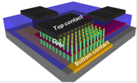 |
| © X-L Han and G. Larrieu Diagram of a 3D nano-transistor showing the gate (red) surrounding the vertical nanowires (green) and separating the contacts at the ends of each nanowire (beige). |
Abstract:
A new breakthrough could push the limits of the miniaturization of electronic components further than previously thought possible. A team at the Laboratoire d'Analyse et d'Architecture des Systčmes (LAAS-CNRS, Toulouse) and Institut d'Électronique, de Microélectronique et de Nanotechnologie (IEMN, CNRS / University of Lille 1 / University of Valenciennes and Hainaut-Cambresis / Isen) has built a nanometric transistor that displays exceptional properties for a device of its size. To achieve this result, the researchers developed a novel three-dimensional architecture consisting of a vertical nanowire array whose conductivity is controlled by a gate measuring only 14 nm in length. Published in Nanoscale, these findings open the way toward alternatives to the planar structures used in microprocessors and memory units. The use of 3D transistors could significantly increase the power of microelectronic devices.
Taking transistors into a new dimension
Paris, France | Posted on March 12th, 2013The "building blocks" of microelectronics, transistors consist of a semiconductor component, called channel, linking two terminals. The flow of current between these terminals is controlled by a third terminal, called gate. Acting like a switch, the gate determines whether the transistor is on or off. Over the past 50 years, transistors have been steadily reduced in size, enabling the development of increasingly powerful microelectronic devices. However, it is generally agreed that today's transistors, with their planar architecture, are nearing the limits of miniaturization: there is a minimum size under which the gate control over the channel becomes less and less effective. In particular, leakage currents begin to interfere with the logical operations performed by the transistor array. To overcome this problem, researchers around the world are investigating alternatives that will allow the race for miniaturization to continue.
A team of researchers at the LAAS and IEMN has now built the first truly three-dimensional nanometric transistor. The device consists of a tight vertical nanowire array of about 200 nm in length linking two conductive surfaces. A chromium gate completely surrounds each nanowire and controls the flow of current, resulting in optimum transistor control for a system of this size. The gate is only 14 nm in length, compared with 28 nm for the transistors in today's chips, but its capacity to control the current in the transistor's channel meets the requirements of contemporary microelectronics.
This architecture could lead to the development of microprocessors in which the transistors are stacked together. The number of transistors in a given space could thus be increased considerably, along with the performance capacity of microprocessors and memory units. Another significant advantage of these components is that they are relatively simple to manufacture and do not require high-resolution lithography.[1] In addition, these 3D transistors could be easily integrated into the conventional microelectronic devices used by the industry today.
A patent has been filed for these transistors. The researchers now plan to continue their efforts to further reduce the size of the gate, which they believe could be made smaller than 10 nm while still providing satisfactory control over the transistor. In addition, the team is looking for industrial partners to help design the electronic devices of the future using the 3D architecture of these novel transistors.
[1] A common technique for surface texturing in micro / nano technology, lithography is used to transfer predefined motifs onto a sensitive resin.
Full bibliographic information
Vertical nanowire array-based field effect transistors for ultimate scaling.. G. Larrieu and X.-L. Han. Nanoscale, online as of 23 January 2013 (doi:10..1039/C3NR33738C).
####
For more information, please click here
Contacts:
Julien Guillaume
+ 33 1 44 96 51 51
Researcher
Guilhem Larrieu
Tel +33 (0)5 61 33 79 84
CNRS press officer
Ornella Piu
Tel +33 (0)1 44 96 43 09
Copyright © AlphaGalileo
If you have a comment, please Contact us.Issuers of news releases, not 7th Wave, Inc. or Nanotechnology Now, are solely responsible for the accuracy of the content.
Bookmark:


| Related News Press |
News and information
![]() Researchers develop molecular qubits that communicate at telecom frequencies October 3rd, 2025
Researchers develop molecular qubits that communicate at telecom frequencies October 3rd, 2025
![]() Next-generation quantum communication October 3rd, 2025
Next-generation quantum communication October 3rd, 2025
![]() "Nanoreactor" cage uses visible light for catalytic and ultra-selective cross-cycloadditions October 3rd, 2025
"Nanoreactor" cage uses visible light for catalytic and ultra-selective cross-cycloadditions October 3rd, 2025
Chip Technology
![]() Lab to industry: InSe wafer-scale breakthrough for future electronics August 8th, 2025
Lab to industry: InSe wafer-scale breakthrough for future electronics August 8th, 2025
![]() A 1960s idea inspires NBI researchers to study hitherto inaccessible quantum states June 6th, 2025
A 1960s idea inspires NBI researchers to study hitherto inaccessible quantum states June 6th, 2025
![]() Programmable electron-induced color router array May 14th, 2025
Programmable electron-induced color router array May 14th, 2025
Nanoelectronics
![]() Lab to industry: InSe wafer-scale breakthrough for future electronics August 8th, 2025
Lab to industry: InSe wafer-scale breakthrough for future electronics August 8th, 2025
![]() Interdisciplinary: Rice team tackles the future of semiconductors Multiferroics could be the key to ultralow-energy computing October 6th, 2023
Interdisciplinary: Rice team tackles the future of semiconductors Multiferroics could be the key to ultralow-energy computing October 6th, 2023
![]() Key element for a scalable quantum computer: Physicists from Forschungszentrum Jülich and RWTH Aachen University demonstrate electron transport on a quantum chip September 23rd, 2022
Key element for a scalable quantum computer: Physicists from Forschungszentrum Jülich and RWTH Aachen University demonstrate electron transport on a quantum chip September 23rd, 2022
![]() Reduced power consumption in semiconductor devices September 23rd, 2022
Reduced power consumption in semiconductor devices September 23rd, 2022
Discoveries
![]() Researchers develop molecular qubits that communicate at telecom frequencies October 3rd, 2025
Researchers develop molecular qubits that communicate at telecom frequencies October 3rd, 2025
![]() Next-generation quantum communication October 3rd, 2025
Next-generation quantum communication October 3rd, 2025
![]() "Nanoreactor" cage uses visible light for catalytic and ultra-selective cross-cycloadditions October 3rd, 2025
"Nanoreactor" cage uses visible light for catalytic and ultra-selective cross-cycloadditions October 3rd, 2025
Announcements
![]() Rice membrane extracts lithium from brines with greater speed, less waste October 3rd, 2025
Rice membrane extracts lithium from brines with greater speed, less waste October 3rd, 2025
![]() Researchers develop molecular qubits that communicate at telecom frequencies October 3rd, 2025
Researchers develop molecular qubits that communicate at telecom frequencies October 3rd, 2025
![]() Next-generation quantum communication October 3rd, 2025
Next-generation quantum communication October 3rd, 2025
![]() "Nanoreactor" cage uses visible light for catalytic and ultra-selective cross-cycloadditions October 3rd, 2025
"Nanoreactor" cage uses visible light for catalytic and ultra-selective cross-cycloadditions October 3rd, 2025
Patents/IP/Tech Transfer/Licensing
![]() Getting drugs across the blood-brain barrier using nanoparticles March 3rd, 2023
Getting drugs across the blood-brain barrier using nanoparticles March 3rd, 2023
![]() Metasurfaces control polarized light at will: New research unlocks the hidden potential of metasurfaces August 13th, 2021
Metasurfaces control polarized light at will: New research unlocks the hidden potential of metasurfaces August 13th, 2021
![]() Arrowhead Pharmaceuticals Announces Closing of Agreement with Takeda November 27th, 2020
Arrowhead Pharmaceuticals Announces Closing of Agreement with Takeda November 27th, 2020
|
|
||
|
|
||
| The latest news from around the world, FREE | ||
|
|
||
|
|
||
| Premium Products | ||
|
|
||
|
Only the news you want to read!
Learn More |
||
|
|
||
|
Full-service, expert consulting
Learn More |
||
|
|
||