Home > Press > Counting the twists in a helical light beam: New device could contribute to a major increase in the rate of future optical communications
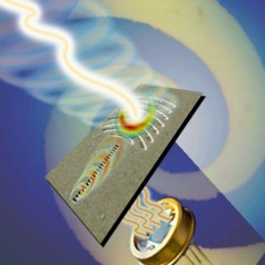 |
| This illustration (not to scale) simulates the process by which an incoming complex wave can be identified and transmitted to a photodetector. (Image courtesy of Patrice Genevet.) |
Abstract:
At a time when communication networks are scrambling for ways to transmit more data over limited bandwidth, a type of twisted light wave is gaining new attention. Called an optical vortex or vortex beam, this complex beam resembles a corkscrew, with waves that rotate as they travel.
Counting the twists in a helical light beam: New device could contribute to a major increase in the rate of future optical communications
Cambridge, MA | Posted on January 8th, 2013Now, applied physicists at the Harvard School of Engineering and Applied Sciences (SEAS) have created a new device that enables a conventional optical detector (which would normally only measure the light's intensity) to pick up on that rotation.
The device, described in the journal Nature Communications, has the potential to add capacity to future optical communication networks.
"Sophisticated optical detectors for vortex beams have been developed before, but they have always been complex, expensive, and bulky," says principal investigator Federico Capasso, Robert L. Wallace Professor of Applied Physics and Vinton Hayes Senior Research Fellow in Electrical Engineering at SEAS.
In contrast, the new device simply adds a metallic pattern to the window of a commercially available, low-cost photodetector. Each pattern is designed to couple with a particular type of incoming vortex beam by matching its orbital angular momentum�the number of twists per wavelength in an optical vortex.
Sensitive to the beam's "twistiness," this new detector can effectively distinguish between different types of vortex beams. Existing communications systems maximize bandwidth by sending many messages simultaneously, each a fraction of a wavelength apart; this is known as wavelength division multiplexing. Vortex beams can add an additional level of multiplexing and therefore should expand the capacity of these systems.
"In recent years, researchers have come to realize that there is a limit to the information transfer rate of about 100 terabits per second per fiber for communication systems that use wavelength division multiplexing to increase the capacity of single-mode optical fibers," explains Capasso. "In the future, this capacity could be greatly increased by using vortex beams transmitted on special multicore or multimode fibers. For a transmission system based on this 'spatial division multiplexing' to provide the extra capacity, special detectors capable of sorting out the type of vortex transmitted will be essential."
The new detector is able to tell one type of vortex beam from another due to its precise nanoscale patterning. When a vortex beam with the correct number of coils per wavelength strikes the gold plating on the detector's surface, it encounters a holographic interference pattern that has been etched into the gold. This nanoscale patterning allows the light to excite the metal's electrons in exactly the right way to produce a focused electromagnetic wave, known as a surface plasmon. The light component of this wave then shines through a series of perforations in the gold, and lands on the photodetector below.
If the incoming light doesn't match the interference pattern, the plasmon beam fails to focus or converge and is blocked from reaching the detector.
Capasso's research team has demonstrated this process using vortex beams with orbital angular momentum of −1, 0, and 1.
"In principle, an array of many different couplers and detectors could be set up to read data transmitted on a very large number of channels," says lead author Patrice Genevet, a research associate in applied physics at SEAS. "With this approach, we transform detectors that were originally only sensitive to the intensity of light, so that they monitor the twist of the wavefronts. More than just detecting a specific twisted beam, our detectors gather additional information on the phase of the light beam."
The device's ability to detect and distinguish vortex beams is important for optical communications, but its capabilities may extend beyond what has been demonstrated.
"Using the same holographic approach, the same device patterned in different ways should be able to couple any type of free-space light beam into any type of surface wave," says Genevet.
Coauthors on this work included Jiao Lin, a former postdoctoral fellow in Capasso's lab (now at the Singapore Institute of Manufacturing Technology), and Harvard graduate student Mikhail A. Kats.
The research was supported by the U.S. Air Force Office of Scientific Research, the U.S. Intelligence Advanced Research Projects Agency, and through research fellowships from the Agency for Science, Technology, and Research in Singapore and the U.S. National Science Foundation (NSF). The researchers also benefited from facilities at Harvard's Center for Nanoscale Systems, a member of the NSF-supported National Nanotechnology Infrastructure Network.
####
For more information, please click here
Contacts:
Caroline Perry
(617) 496-1351
Copyright © Harvard's School of Engineering and Applied Sciences (SEAS)
If you have a comment, please Contact us.Issuers of news releases, not 7th Wave, Inc. or Nanotechnology Now, are solely responsible for the accuracy of the content.
Bookmark:


| Related News Press |
News and information
![]() Simulating magnetization in a Heisenberg quantum spin chain April 5th, 2024
Simulating magnetization in a Heisenberg quantum spin chain April 5th, 2024
![]() NRL charters Navy�s quantum inertial navigation path to reduce drift April 5th, 2024
NRL charters Navy�s quantum inertial navigation path to reduce drift April 5th, 2024
![]() Discovery points path to flash-like memory for storing qubits: Rice find could hasten development of nonvolatile quantum memory April 5th, 2024
Discovery points path to flash-like memory for storing qubits: Rice find could hasten development of nonvolatile quantum memory April 5th, 2024
Govt.-Legislation/Regulation/Funding/Policy
![]() NRL charters Navy�s quantum inertial navigation path to reduce drift April 5th, 2024
NRL charters Navy�s quantum inertial navigation path to reduce drift April 5th, 2024
![]() Discovery points path to flash-like memory for storing qubits: Rice find could hasten development of nonvolatile quantum memory April 5th, 2024
Discovery points path to flash-like memory for storing qubits: Rice find could hasten development of nonvolatile quantum memory April 5th, 2024
![]() Chemical reactions can scramble quantum information as well as black holes April 5th, 2024
Chemical reactions can scramble quantum information as well as black holes April 5th, 2024
Optical computing/Photonic computing
![]() With VECSELs towards the quantum internet Fraunhofer: IAF achieves record output power with VECSEL for quantum frequency converters April 5th, 2024
With VECSELs towards the quantum internet Fraunhofer: IAF achieves record output power with VECSEL for quantum frequency converters April 5th, 2024
![]() Chemical reactions can scramble quantum information as well as black holes April 5th, 2024
Chemical reactions can scramble quantum information as well as black holes April 5th, 2024
![]() Optically trapped quantum droplets of light can bind together to form macroscopic complexes March 8th, 2024
Optically trapped quantum droplets of light can bind together to form macroscopic complexes March 8th, 2024
![]() HKUST researchers develop new integration technique for efficient coupling of III-V and silicon February 16th, 2024
HKUST researchers develop new integration technique for efficient coupling of III-V and silicon February 16th, 2024
Discoveries
![]() Chemical reactions can scramble quantum information as well as black holes April 5th, 2024
Chemical reactions can scramble quantum information as well as black holes April 5th, 2024
![]() New micromaterial releases nanoparticles that selectively destroy cancer cells April 5th, 2024
New micromaterial releases nanoparticles that selectively destroy cancer cells April 5th, 2024
![]() Utilizing palladium for addressing contact issues of buried oxide thin film transistors April 5th, 2024
Utilizing palladium for addressing contact issues of buried oxide thin film transistors April 5th, 2024
Announcements
![]() NRL charters Navy�s quantum inertial navigation path to reduce drift April 5th, 2024
NRL charters Navy�s quantum inertial navigation path to reduce drift April 5th, 2024
![]() Discovery points path to flash-like memory for storing qubits: Rice find could hasten development of nonvolatile quantum memory April 5th, 2024
Discovery points path to flash-like memory for storing qubits: Rice find could hasten development of nonvolatile quantum memory April 5th, 2024
Tools
![]() Ferroelectrically modulate the Fermi level of graphene oxide to enhance SERS response November 3rd, 2023
Ferroelectrically modulate the Fermi level of graphene oxide to enhance SERS response November 3rd, 2023
![]() The USTC realizes In situ electron paramagnetic resonance spectroscopy using single nanodiamond sensors November 3rd, 2023
The USTC realizes In situ electron paramagnetic resonance spectroscopy using single nanodiamond sensors November 3rd, 2023
Military
![]() NRL charters Navy�s quantum inertial navigation path to reduce drift April 5th, 2024
NRL charters Navy�s quantum inertial navigation path to reduce drift April 5th, 2024
![]() What heat can tell us about battery chemistry: using the Peltier effect to study lithium-ion cells March 8th, 2024
What heat can tell us about battery chemistry: using the Peltier effect to study lithium-ion cells March 8th, 2024
![]() New chip opens door to AI computing at light speed February 16th, 2024
New chip opens door to AI computing at light speed February 16th, 2024
Photonics/Optics/Lasers
![]() With VECSELs towards the quantum internet Fraunhofer: IAF achieves record output power with VECSEL for quantum frequency converters April 5th, 2024
With VECSELs towards the quantum internet Fraunhofer: IAF achieves record output power with VECSEL for quantum frequency converters April 5th, 2024
![]() Nanoscale CL thermometry with lanthanide-doped heavy-metal oxide in TEM March 8th, 2024
Nanoscale CL thermometry with lanthanide-doped heavy-metal oxide in TEM March 8th, 2024
![]() Optically trapped quantum droplets of light can bind together to form macroscopic complexes March 8th, 2024
Optically trapped quantum droplets of light can bind together to form macroscopic complexes March 8th, 2024
![]() HKUST researchers develop new integration technique for efficient coupling of III-V and silicon February 16th, 2024
HKUST researchers develop new integration technique for efficient coupling of III-V and silicon February 16th, 2024
|
|
||
|
|
||
| The latest news from around the world, FREE | ||
|
|
||
|
|
||
| Premium Products | ||
|
|
||
|
Only the news you want to read!
Learn More |
||
|
|
||
|
Full-service, expert consulting
Learn More |
||
|
|
||