Home > Press > PTB measurements for the next computer chip generation: Cooperation between Carl Zeiss and PTB on EUV lithography extended
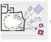 |
| Beamlines and instrumentation at the Metrology Light Source (MLS). (EUV beamline: #3; set-up for the calibration of radiation sources: #2b; undulator beamline: #1d; infrared beamline: #6) (Image: PTB) |
Abstract:
European companies are the world leaders in the development of EUV lithography for the manufacture of semiconductor chips with even shorter wavelengths than up to now, i.e. with 13.5 nanometres in the spectral range of the so-called "Extreme UV (EUV)". The volume production of lens systems and wafer scanners of EU lithography (EUVL) is planned for 2014. In this development, the Physikalisch-Technische Bundesanstalt (PTB) is at the fore. With a new EUV beamline at PTB's own electron storage ring - the Metrology Light Source (MLS) in Berlin-Adlershof - it will characterize EUVL lens systems for this purpose. The cooperation with Carl Zeiss SMT GmbH, which has been running since 1998, has now been extended for another four years. PTB measurements will help to give proof of the quality of the Zeiss lens systems in the so-called "steppers" (lithography machines) of the Dutch company ASML, the global market leader in this field.
PTB measurements for the next computer chip generation: Cooperation between Carl Zeiss and PTB on EUV lithography extended
Braunschweig , Germany | Posted on December 2nd, 2012The combination is unique worldwide: although there are a number of electron storage rings, and although a national metrology institute exists in almost every country as the highest authority in the field of measurements, only the Physikalisch-Technische Bundesanstalt has its own modern electron storage ring - the Metrology Light Source - and the measurement arrangements required for the high-precision characterization of EUVL lens systems. The MLS has been operated since 2008; it furnishes synchrotron radiation from the terahertz range up to the EUV range and has clearly extended PTB's measurement capabilities at the nearby electron storage ring BESSY II, where it uses X-rays on a large scale for the various metrological tasks.
The new EUV beamline is particularly suited for the investigation of photodetectors and structured optical elements and has - after the commissioning phase - been increasingly used since the beginning of this year for measurements within the scope of research cooperations, in particular for EUVL. "Our greatest strength - which is very well received by the cooperation partners - consists in the so-called "At-wavelength measurements". We characterize the lens systems at the EUVL working wavelength - and not only with visible light. Our measurements therefore directly describe the behaviour of lens systems in the production machines", explains Frank Scholze, head of the PTB working group.
The great demand from industry had induced PTB to develop its measurement capabilities at the two storage rings even further. In mid-2013, the large EUV reflectometer of BESSY II is to move to the MLS. In its place, an EUV scatterometer/ellipsometer will be installed which has been particularly suited for scatter experiments. Then, at the latest, a total of approximately 6000 hours of synchrotron radiation measuring time per year will be available to PTB for EUV metrology.
Also in other areas, PTB has clearly extended the field of "metrology with synchrotron radiation" by the commissioning of new beamlines at the MLS. Compared to its predecessor at BESSY II, a new measuring set-up for the calibration of radiation sources now also allows measurements to be carried out at wavelengths below 40 nm. Calibrated radiation sources in the vacuum-UV (VUV) and the EUV are, for example, of great importance for the characterization of space telescopes for solar and atmospheric research. In addition, the new undulator beamline provides monochromatized intensive and profoundly polarized radiation from the IR range up to the EUV range. At present, the first quantitative investigations of surfaces are being carried out by means of UV/VUV ellipsometry and electron spectroscopy together with partners from the research site Adlershof. Furthermore, a new near-field microscope has been put into operation at the infrared beamline of the MLS.
####
About Physikalisch-Technische Bundesanstalt (PTB)
PTB is the German national metrology institute providing scientific and technical services. PTB measures with the highest accuracy and reliability � metrology as the core competence
For more information, please click here
Contacts:
Dr. Frank Scholze
PTB Working Group 7.12
EUV Radiometry
Phone: +49(30) 3481-7120
Copyright © AlphaGalileo
If you have a comment, please Contact us.Issuers of news releases, not 7th Wave, Inc. or Nanotechnology Now, are solely responsible for the accuracy of the content.
Bookmark:


| Related News Press |
News and information
![]() Simulating magnetization in a Heisenberg quantum spin chain April 5th, 2024
Simulating magnetization in a Heisenberg quantum spin chain April 5th, 2024
![]() NRL charters Navy�s quantum inertial navigation path to reduce drift April 5th, 2024
NRL charters Navy�s quantum inertial navigation path to reduce drift April 5th, 2024
![]() Discovery points path to flash-like memory for storing qubits: Rice find could hasten development of nonvolatile quantum memory April 5th, 2024
Discovery points path to flash-like memory for storing qubits: Rice find could hasten development of nonvolatile quantum memory April 5th, 2024
Imaging
![]() Nanoscale CL thermometry with lanthanide-doped heavy-metal oxide in TEM March 8th, 2024
Nanoscale CL thermometry with lanthanide-doped heavy-metal oxide in TEM March 8th, 2024
Laboratories
![]() A battery�s hopping ions remember where they�ve been: Seen in atomic detail, the seemingly smooth flow of ions through a battery�s electrolyte is surprisingly complicated February 16th, 2024
A battery�s hopping ions remember where they�ve been: Seen in atomic detail, the seemingly smooth flow of ions through a battery�s electrolyte is surprisingly complicated February 16th, 2024
![]() NRL discovers two-dimensional waveguides February 16th, 2024
NRL discovers two-dimensional waveguides February 16th, 2024
Chip Technology
![]() Discovery points path to flash-like memory for storing qubits: Rice find could hasten development of nonvolatile quantum memory April 5th, 2024
Discovery points path to flash-like memory for storing qubits: Rice find could hasten development of nonvolatile quantum memory April 5th, 2024
![]() Utilizing palladium for addressing contact issues of buried oxide thin film transistors April 5th, 2024
Utilizing palladium for addressing contact issues of buried oxide thin film transistors April 5th, 2024
![]() HKUST researchers develop new integration technique for efficient coupling of III-V and silicon February 16th, 2024
HKUST researchers develop new integration technique for efficient coupling of III-V and silicon February 16th, 2024
Announcements
![]() NRL charters Navy�s quantum inertial navigation path to reduce drift April 5th, 2024
NRL charters Navy�s quantum inertial navigation path to reduce drift April 5th, 2024
![]() Discovery points path to flash-like memory for storing qubits: Rice find could hasten development of nonvolatile quantum memory April 5th, 2024
Discovery points path to flash-like memory for storing qubits: Rice find could hasten development of nonvolatile quantum memory April 5th, 2024
Tools
![]() Ferroelectrically modulate the Fermi level of graphene oxide to enhance SERS response November 3rd, 2023
Ferroelectrically modulate the Fermi level of graphene oxide to enhance SERS response November 3rd, 2023
![]() The USTC realizes In situ electron paramagnetic resonance spectroscopy using single nanodiamond sensors November 3rd, 2023
The USTC realizes In situ electron paramagnetic resonance spectroscopy using single nanodiamond sensors November 3rd, 2023
Alliances/Trade associations/Partnerships/Distributorships
![]() Chicago Quantum Exchange welcomes six new partners highlighting quantum technology solutions, from Chicago and beyond September 23rd, 2022
Chicago Quantum Exchange welcomes six new partners highlighting quantum technology solutions, from Chicago and beyond September 23rd, 2022
![]() University of Illinois Chicago joins Brookhaven Lab's Quantum Center June 10th, 2022
University of Illinois Chicago joins Brookhaven Lab's Quantum Center June 10th, 2022
|
|
||
|
|
||
| The latest news from around the world, FREE | ||
|
|
||
|
|
||
| Premium Products | ||
|
|
||
|
Only the news you want to read!
Learn More |
||
|
|
||
|
Full-service, expert consulting
Learn More |
||
|
|
||