Home > Press > First 3D Nanoscale Optical Cavities from Metamaterials: Berkeley Lab Development Holds Promise for Nanolasers, LEDs, Optical Sensors and Photonic Communications
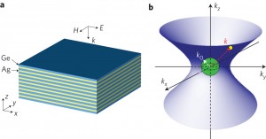 |
| This schematic shows (a) an indefinite metamaterial structure with alternating silver and germanium multilayers; and (b) its iso-frequency contour of light wave vectors with negative refractions along the x- and y-directions, and positive along the z-direction. (Courtesy of Xiang Zhang group) |
Abstract:
The world's smallest three-dimensional optical cavities with the potential to generate the world's most intense nanolaser beams have been created by a scientific team led by researchers with the U.S. Department of Energy (DOE)'s Lawrence Berkeley National Laboratory (Berkeley Lab) and the University of California (UC) Berkeley. In addition to nanolasers, these unique optical cavities with their extraordinary electromagnetic properties should be applicable to a broad range of other technologies, including LEDs, optical sensing, nonlinear optics, quantum optics and photonic integrated circuits.
First 3D Nanoscale Optical Cavities from Metamaterials: Berkeley Lab Development Holds Promise for Nanolasers, LEDs, Optical Sensors and Photonic Communications
Berkeley, CA | Posted on June 27th, 2012By alternating super-thin multiple layers of silver and germanium, the researchers fabricated an "indefinite metamaterial" from which they created their 3D optical cavities. In natural materials, light behaves the same no matter what direction it propagates. In indefinite metamaterials, light can actually be bent backwards in some directions, a property known as negative refraction. The use of this indefinite metamaterial enabled the scaling down of the 3D optical cavities to extremely deep subwavelength (nanometer) size, resulting in a "hyperboloid iso-frequency contour" of light wave vectors (a measure of magnitude and direction) that supported the highest optical refractive indices ever reported.
This study was directed by Xiang Zhang, a principal investigator with Berkeley Lab's Materials Sciences Division and director of UC Berkeley's Nano-scale Science and Engineering Center (SINAM). He is the corresponding author of a paper describing this research titled "Experimental realization of three-dimensional indefinite cavities at the nanoscale with an anomalous scaling law," which has been published in the journal Nature Photonics. Co-authoring this paper with Zhang were Xiaodong Yang, Jie Yao, Junsuk Rho and Xiaobo Yin.
"Our work opens up a new approach for designing a truly nano-scale optical cavity," Zhang says. "By using metamaterials, we show intriguing cavity physics that counters conventional wisdom. For example, the quality factor of our optical mode rapidly increases with the decrease of cavity size. The results of this study provide us with a tremendous opportunity to develop high performance photonic devices for communications."
Optical cavities are the major components of most lasers. Light confined within an optical cavity will be reflected back and forth between two opposing mirrors to produce a standing wave at a specific resonant frequency. It is from this standing light wave that a laser beam is generated. Optical cavities made from natural materials can be no smaller than the wavelength of the light propagating through them. Metamaterials, however, allow for electromagnetic behavior that is not attainable in nature. Engineered from a combination of metals and dielectrics - insulators that become polarized in the presence of an electromagnetic field - metamaterials derive their optical properties from their structure rather than their chemical composition, as is the case with natural optical materials.
"Due to the unnaturally high refractive index supported in the metamaterials, our 3D cavities can be smaller than one tenth of the optical wavelength," says Xiaodong Yang, lead author of the Nature Photonics paper who is now with the Missouri University of Science and Technology. "At these nanoscale dimensions, optical cavities compress the optical mode into a tiny space, increasing the photon density of states and thereby enhancing the interactions between light and matter."
Another advantage of using indefinite metamaterials to make their 3D optical cavities, Yang says, is that cavities with different sizes can have the same resonance frequency, providing more flexibility in the optical cavity design. Another advantage is that the photons lost when light is reflected back and forth - a problem for optical cavities from natural materials - is reduced as the cavity size gets smaller. Yang says this will benefit the design of future nanoscale lasers.
Germanium was the dielectric chosen to make this metamaterial because it has a relatively high refractive index (about 4.0), compared to air (1.0), which is the dielectric most typically used to make a metamaterial. The alternating layers of silver (20 nanometers thick) and germanium (30 nanometers thick) were cut into cubes of various sizes, depending on the number of metal/dielectric layers. The cube walls tilt into the shape of a trapezoid during the final stage of fabrication with a nano-sized optical cavity in the core.
"The hyperboloid iso-frequency contour of wave vector space in these cavities allowed us to reach very high wave vector values, Yang says. "As wave vector values are proportional to the refractive index, we were able to record optical refractive indices as large as 17.4, which is far beyond that found in natural materials."
This research was supported by the U.S. Department of Air Force Office of Scientific Research.
####
About DOE/Lawrence Berkeley National Laboratory
Lawrence Berkeley National Laboratory addresses the world�s most urgent scientific challenges by advancing sustainable energy, protecting human health, creating new materials, and revealing the origin and fate of the universe. Founded in 1931, Berkeley Lab�s scientific expertise has been recognized with 13 Nobel prizes. The University of California manages Berkeley Lab for the U.S. Department of Energy�s Office of Science. For more, visit www.lbl.gov.
For more information, please click here
Contacts:
Lynn Yarris
(510) 486-5375
Copyright © DOE/Lawrence Berkeley National Laboratory
If you have a comment, please Contact us.Issuers of news releases, not 7th Wave, Inc. or Nanotechnology Now, are solely responsible for the accuracy of the content.
Bookmark:


| Related Links |
![]() For more information about the research of Xiang Zhang visit:
For more information about the research of Xiang Zhang visit:
| Related News Press |
News and information
![]() Simulating magnetization in a Heisenberg quantum spin chain April 5th, 2024
Simulating magnetization in a Heisenberg quantum spin chain April 5th, 2024
![]() NRL charters Navy�s quantum inertial navigation path to reduce drift April 5th, 2024
NRL charters Navy�s quantum inertial navigation path to reduce drift April 5th, 2024
![]() Discovery points path to flash-like memory for storing qubits: Rice find could hasten development of nonvolatile quantum memory April 5th, 2024
Discovery points path to flash-like memory for storing qubits: Rice find could hasten development of nonvolatile quantum memory April 5th, 2024
Laboratories
![]() A battery�s hopping ions remember where they�ve been: Seen in atomic detail, the seemingly smooth flow of ions through a battery�s electrolyte is surprisingly complicated February 16th, 2024
A battery�s hopping ions remember where they�ve been: Seen in atomic detail, the seemingly smooth flow of ions through a battery�s electrolyte is surprisingly complicated February 16th, 2024
![]() NRL discovers two-dimensional waveguides February 16th, 2024
NRL discovers two-dimensional waveguides February 16th, 2024
![]() Three-pronged approach discerns qualities of quantum spin liquids November 17th, 2023
Three-pronged approach discerns qualities of quantum spin liquids November 17th, 2023
Govt.-Legislation/Regulation/Funding/Policy
![]() NRL charters Navy�s quantum inertial navigation path to reduce drift April 5th, 2024
NRL charters Navy�s quantum inertial navigation path to reduce drift April 5th, 2024
![]() Discovery points path to flash-like memory for storing qubits: Rice find could hasten development of nonvolatile quantum memory April 5th, 2024
Discovery points path to flash-like memory for storing qubits: Rice find could hasten development of nonvolatile quantum memory April 5th, 2024
![]() Chemical reactions can scramble quantum information as well as black holes April 5th, 2024
Chemical reactions can scramble quantum information as well as black holes April 5th, 2024
Discoveries
![]() Chemical reactions can scramble quantum information as well as black holes April 5th, 2024
Chemical reactions can scramble quantum information as well as black holes April 5th, 2024
![]() New micromaterial releases nanoparticles that selectively destroy cancer cells April 5th, 2024
New micromaterial releases nanoparticles that selectively destroy cancer cells April 5th, 2024
![]() Utilizing palladium for addressing contact issues of buried oxide thin film transistors April 5th, 2024
Utilizing palladium for addressing contact issues of buried oxide thin film transistors April 5th, 2024
Announcements
![]() NRL charters Navy�s quantum inertial navigation path to reduce drift April 5th, 2024
NRL charters Navy�s quantum inertial navigation path to reduce drift April 5th, 2024
![]() Discovery points path to flash-like memory for storing qubits: Rice find could hasten development of nonvolatile quantum memory April 5th, 2024
Discovery points path to flash-like memory for storing qubits: Rice find could hasten development of nonvolatile quantum memory April 5th, 2024
Tools
![]() Ferroelectrically modulate the Fermi level of graphene oxide to enhance SERS response November 3rd, 2023
Ferroelectrically modulate the Fermi level of graphene oxide to enhance SERS response November 3rd, 2023
![]() The USTC realizes In situ electron paramagnetic resonance spectroscopy using single nanodiamond sensors November 3rd, 2023
The USTC realizes In situ electron paramagnetic resonance spectroscopy using single nanodiamond sensors November 3rd, 2023
Military
![]() NRL charters Navy�s quantum inertial navigation path to reduce drift April 5th, 2024
NRL charters Navy�s quantum inertial navigation path to reduce drift April 5th, 2024
![]() What heat can tell us about battery chemistry: using the Peltier effect to study lithium-ion cells March 8th, 2024
What heat can tell us about battery chemistry: using the Peltier effect to study lithium-ion cells March 8th, 2024
![]() New chip opens door to AI computing at light speed February 16th, 2024
New chip opens door to AI computing at light speed February 16th, 2024
Photonics/Optics/Lasers
![]() With VECSELs towards the quantum internet Fraunhofer: IAF achieves record output power with VECSEL for quantum frequency converters April 5th, 2024
With VECSELs towards the quantum internet Fraunhofer: IAF achieves record output power with VECSEL for quantum frequency converters April 5th, 2024
![]() Nanoscale CL thermometry with lanthanide-doped heavy-metal oxide in TEM March 8th, 2024
Nanoscale CL thermometry with lanthanide-doped heavy-metal oxide in TEM March 8th, 2024
![]() Optically trapped quantum droplets of light can bind together to form macroscopic complexes March 8th, 2024
Optically trapped quantum droplets of light can bind together to form macroscopic complexes March 8th, 2024
![]() HKUST researchers develop new integration technique for efficient coupling of III-V and silicon February 16th, 2024
HKUST researchers develop new integration technique for efficient coupling of III-V and silicon February 16th, 2024
Research partnerships
![]() Discovery points path to flash-like memory for storing qubits: Rice find could hasten development of nonvolatile quantum memory April 5th, 2024
Discovery points path to flash-like memory for storing qubits: Rice find could hasten development of nonvolatile quantum memory April 5th, 2024
![]() Researchers� approach may protect quantum computers from attacks March 8th, 2024
Researchers� approach may protect quantum computers from attacks March 8th, 2024
![]() 'Sudden death' of quantum fluctuations defies current theories of superconductivity: Study challenges the conventional wisdom of superconducting quantum transitions January 12th, 2024
'Sudden death' of quantum fluctuations defies current theories of superconductivity: Study challenges the conventional wisdom of superconducting quantum transitions January 12th, 2024
|
|
||
|
|
||
| The latest news from around the world, FREE | ||
|
|
||
|
|
||
| Premium Products | ||
|
|
||
|
Only the news you want to read!
Learn More |
||
|
|
||
|
Full-service, expert consulting
Learn More |
||
|
|
||