Home > Press > Success of 3D NanoCompass will enable Baolab to create low cost, smart, reconfigurable Inertial Measurement Unit
 |
Abstract:
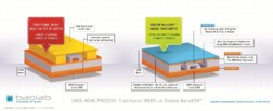
Baolab Microsystems has announced that it expects to be able to modify the structures that it designed for its 3D NanoCompass™ to build a range of other motion sensors and, ultimately, to create low cost, smart, reconfigurable Inertial Measurement Units (IMUs). These NanoIMUs™ will use Baolab's patented, award winning NanoEMS™ technology to create nanoscale MEMS (Micro Electro Mechanical Systems) within the standard metal structure of a high volume manufactured CMOS wafer.
Success of 3D NanoCompass will enable Baolab to create low cost, smart, reconfigurable Inertial Measurement Unit
Barcelona, Spain | Posted on May 8th, 2012"We have designed ways to modify the structure that we developed for the 3D NanoCompass so that it can be used to create gyroscopes and accelerometers as well as magnetometers" explained Dave Doyle, Baolab's CEO. "As we have the ability to build combinations of these different types of sensors simultaneously on the same chip along with the associated electronics to provide control and intelligence, we will be able to create the product that the industry is wanting - multi-sensor IMUs that can be activated and configured dynamically as required by the application. The key is that our technology enables us to build MEMS using standard CMOS production techniques so we can make as many as we like of whatever mix of sensors that are required at the same time, integrated with the analog and digital electronics running fusion software to make them smart."
The traditional way of making MEMS sensors requires a different production process to make each type of sensor. Baolab's NanoEMS approach will enable the costs of making smart, multi-sensor IMUs to be slashed dramatically, accelerating the drive to provide ubiquitous multi-sensor awareness into almost any device for enhanced performance and features.
"We have proved that we have solved all the challenges of making MEMS within the CMOS wafer with our production of working 3D NanoCompasses," added Dave Doyle. "We will be introducing a series of nanosensor products as we work our way through the roadmap towards our goal of ultra low cost, smart, multi-sensor NanoIMUs."
####
About Baolab Microsystems
Baolab has developed an innovative technology called NanoEMS™ that enables MEMS to be created inside the CMOS wafer using standard manufacturing techniques. This enables them to be made an order of magnitude smaller than existing techniques of building MEMS on the surface of the wafer and also at a fraction of the cost. Privately owned, Baolab is based in Barcelona, Spain.
NanoIMU, NanoEMS and 3D NanoCompass are trademarks of Baolab Microsystems, S.L.
For more information, please click here
Contacts:
Nigel Robson
+44 1481 233080
Vortex PR
Tel: +34-93-394-17-70
Copyright © Baolab Microsystems
If you have a comment, please Contact us.Issuers of news releases, not 7th Wave, Inc. or Nanotechnology Now, are solely responsible for the accuracy of the content.
Bookmark:


| Related News Press |
News and information
![]() Quantum computer improves AI predictions April 17th, 2026
Quantum computer improves AI predictions April 17th, 2026
![]() Flexible sensor gains sensitivity under pressure April 17th, 2026
Flexible sensor gains sensitivity under pressure April 17th, 2026
![]() A reusable chip for particulate matter sensing April 17th, 2026
A reusable chip for particulate matter sensing April 17th, 2026
![]() Detecting vibrational quantum beating in the predissociation dynamics of SF6 using time-resolved photoelectron spectroscopy April 17th, 2026
Detecting vibrational quantum beating in the predissociation dynamics of SF6 using time-resolved photoelectron spectroscopy April 17th, 2026
MEMS
Chip Technology
![]() A reusable chip for particulate matter sensing April 17th, 2026
A reusable chip for particulate matter sensing April 17th, 2026
![]() Metasurfaces smooth light to boost magnetic sensing precision January 30th, 2026
Metasurfaces smooth light to boost magnetic sensing precision January 30th, 2026
Sensors
![]() Flexible sensor gains sensitivity under pressure April 17th, 2026
Flexible sensor gains sensitivity under pressure April 17th, 2026
![]() Tiny nanosheets, big leap: A new sensor detects ethanol at ultra-low levels January 30th, 2026
Tiny nanosheets, big leap: A new sensor detects ethanol at ultra-low levels January 30th, 2026
![]() From sensors to smart systems: the rise of AI-driven photonic noses January 30th, 2026
From sensors to smart systems: the rise of AI-driven photonic noses January 30th, 2026
![]() Sensors innovations for smart lithium-based batteries: advancements, opportunities, and potential challenges August 8th, 2025
Sensors innovations for smart lithium-based batteries: advancements, opportunities, and potential challenges August 8th, 2025
Announcements
![]() A fundamentally new therapeutic approach to cystic fibrosis: Nanobody repairs cellular defect April 17th, 2026
A fundamentally new therapeutic approach to cystic fibrosis: Nanobody repairs cellular defect April 17th, 2026
![]() UC Irvine physicists discover method to reverse ‘quantum scrambling’ : The work addresses the problem of information loss in quantum computing system April 17th, 2026
UC Irvine physicists discover method to reverse ‘quantum scrambling’ : The work addresses the problem of information loss in quantum computing system April 17th, 2026
|
|
||
|
|
||
| The latest news from around the world, FREE | ||
|
|
||
|
|
||
| Premium Products | ||
|
|
||
|
Only the news you want to read!
Learn More |
||
|
|
||
|
Full-service, expert consulting
Learn More |
||
|
|
||