Home > Press > 3D Laser Lithography System Employs XYZ Nano-Positioning Stage
 |
Abstract:
Piezo nano-positioning systems specialist PI (Physik Instrumente) provides a 3-axis nano-positioning stage that is employed in a novel laser lithography system by Nanoscribe GmbH. The lithography system can produce complex 3-dimensional structures, fully automatic and repeatable with a precision and flexibility previously unavailable. Sub-micron structures with sizes of up to 1 mm und widths to 150 nm are feasible
3D Laser Lithography System Employs XYZ Nano-Positioning Stage
Auburn, MA | Posted on April 16th, 2012Piezo: The driving Force
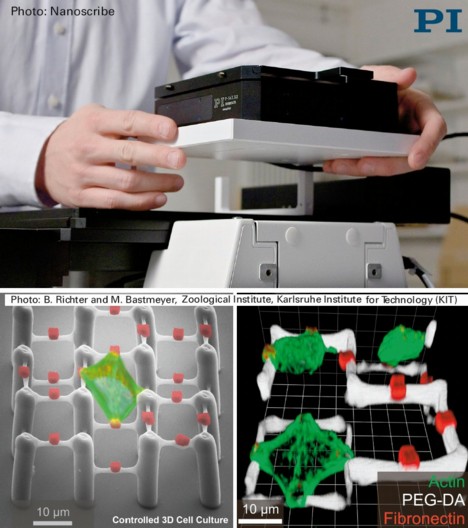
The driving force of Nanoscribe's laser lithography system is a PImars P-563 flexure-guided, piezo-driven nanopositioning XYZ stage from PI. It provides positioning ranges to 300x300x300 microns and nanometer scale repeatability. A parallel-metrology position feedback system based on highly linear capacitive sensors is integrated and allows the sample to be moved precisely and repeatedly in relation to the laser focus. A digital piezo motion controller provides the necessary path control on a nanometric scale.
The high accuracy and fast response of the piezoelectric nano positioning stage makes it possible to equip surfaces with particular biometric characteristics or to create microstructures for small pumps and needles.. Typical applications for 3D laser lithography are the creation of three-dimensional structures for cell biology.
More information on laser lithography for cell biology www.nanopositioning.net/Nanopositioning_For_Biotechnology.htm
More information on XYZ piezo nano-positioning systems
www.nanopositioning.net/XYZ_nanopositioning_stage.php#P563
####
About PI (Physik Instrumente)
PI is a leading manufacturer of precision motion control equipment, piezo systems, piezo motors and actuators for medical engineering, photonics, bio-nano-technology, & semiconductor applications. PI has been developing and manufacturing standard & custom precision products with piezoceramic and electromagnetic drives for 4 decades. The company has been ISO 9001 certified since 1994 and provides innovative, high-quality solutions for OEM and research. PI is present worldwide with eight subsidiaries, R&D / engineering on 3 continents and total staff of 700+
PI USA designs and manufactures piezo products at the company�s US headquarters in Auburn, MA.
For more information, please click here
Contacts:
USA / Canada:
www.pi-usa.us
East:
Tel: (508) 832-3456
Midwest
(508) 832-3456
West
Tel: (949) 679-9191
Europe: www.pi.ws
Germany: +49 (721) 4846-0
Italy: +39 (02) 665 011 01
France: +33 (1) 481 039 30
UK: +44 (1582) 764 334
Asia:
www.pi-japan.jp
www.pi-singapore.sg
www.pikorea.co.kr/
www.pi-china.cn
Stefan Vorndran
VP Marketing
-----------------------------
PI (Physik Instrumente) L.P.
16 Albert St.
Auburn, MA 01501
email:
Tel: 508-832-3456,
Fax: 508-832-0506
www.pi.ws
www.pi-usa.us
Copyright © PI (Physik Instrumente)
If you have a comment, please Contact us.Issuers of news releases, not 7th Wave, Inc. or Nanotechnology Now, are solely responsible for the accuracy of the content.
Bookmark:


| Related News Press |
News and information
![]() Simulating magnetization in a Heisenberg quantum spin chain April 5th, 2024
Simulating magnetization in a Heisenberg quantum spin chain April 5th, 2024
![]() NRL charters Navy�s quantum inertial navigation path to reduce drift April 5th, 2024
NRL charters Navy�s quantum inertial navigation path to reduce drift April 5th, 2024
![]() Discovery points path to flash-like memory for storing qubits: Rice find could hasten development of nonvolatile quantum memory April 5th, 2024
Discovery points path to flash-like memory for storing qubits: Rice find could hasten development of nonvolatile quantum memory April 5th, 2024
Announcements
![]() NRL charters Navy�s quantum inertial navigation path to reduce drift April 5th, 2024
NRL charters Navy�s quantum inertial navigation path to reduce drift April 5th, 2024
![]() Discovery points path to flash-like memory for storing qubits: Rice find could hasten development of nonvolatile quantum memory April 5th, 2024
Discovery points path to flash-like memory for storing qubits: Rice find could hasten development of nonvolatile quantum memory April 5th, 2024
Tools
![]() Ferroelectrically modulate the Fermi level of graphene oxide to enhance SERS response November 3rd, 2023
Ferroelectrically modulate the Fermi level of graphene oxide to enhance SERS response November 3rd, 2023
![]() The USTC realizes In situ electron paramagnetic resonance spectroscopy using single nanodiamond sensors November 3rd, 2023
The USTC realizes In situ electron paramagnetic resonance spectroscopy using single nanodiamond sensors November 3rd, 2023
Photonics/Optics/Lasers
![]() With VECSELs towards the quantum internet Fraunhofer: IAF achieves record output power with VECSEL for quantum frequency converters April 5th, 2024
With VECSELs towards the quantum internet Fraunhofer: IAF achieves record output power with VECSEL for quantum frequency converters April 5th, 2024
![]() Nanoscale CL thermometry with lanthanide-doped heavy-metal oxide in TEM March 8th, 2024
Nanoscale CL thermometry with lanthanide-doped heavy-metal oxide in TEM March 8th, 2024
![]() Optically trapped quantum droplets of light can bind together to form macroscopic complexes March 8th, 2024
Optically trapped quantum droplets of light can bind together to form macroscopic complexes March 8th, 2024
![]() HKUST researchers develop new integration technique for efficient coupling of III-V and silicon February 16th, 2024
HKUST researchers develop new integration technique for efficient coupling of III-V and silicon February 16th, 2024
Printing/Lithography/Inkjet/Inks/Bio-printing/Dyes
![]() Presenting: Ultrasound-based printing of 3D materials�potentially inside the body December 8th, 2023
Presenting: Ultrasound-based printing of 3D materials�potentially inside the body December 8th, 2023
![]() Simple ballpoint pen can write custom LEDs August 11th, 2023
Simple ballpoint pen can write custom LEDs August 11th, 2023
![]() Disposable electronics on a simple sheet of paper October 7th, 2022
Disposable electronics on a simple sheet of paper October 7th, 2022
|
|
||
|
|
||
| The latest news from around the world, FREE | ||
|
|
||
|
|
||
| Premium Products | ||
|
|
||
|
Only the news you want to read!
Learn More |
||
|
|
||
|
Full-service, expert consulting
Learn More |
||
|
|
||