Home > Press > New Microscope at Brookhaven Lab Promises Unprecedented Experimental Opportunities in Materials Science
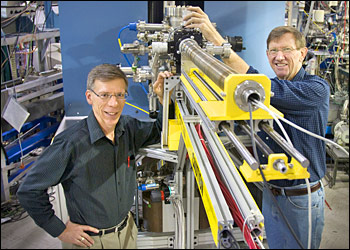 |
| Dan Fischer (left) and Raymond Browning show off the prototype of the Vector Potential Photoelectron Microscope. |
Abstract:
A new class of x-ray photoelectron spectroscopic microscope has been developed at the U.S. Department of Energy's (DOE) Brookhaven National Laboratory. The microscope will be used for advanced research on a wide range of technologically important materials systems. This new class of microscope was invented by Raymond Browning, of R. Browning Consultants and funded by National Institute of Standards and Technology (NIST) Small Business Innovation and Research (SBIR) contracts. A prototype of the new instrument, a Vector Potential Photoelectron Microscope (VPPEM), has been built in collaboration with the NIST Synchrotron Methods Group at the Laboratory's National Synchrotron Light Source (NSLS).
New Microscope at Brookhaven Lab Promises Unprecedented Experimental Opportunities in Materials Science
Upton, NY | Posted on November 29th, 2011The new microscope uses a unique imaging method, and opens up many novel experimental possibilities. According to Browning, VPPEM potentially has a thousand times greater spatial resolution than current technology can provide, and is expected to be the world's most advanced general purpose x-ray photoelectron microscope when combined with NIST's beamline at Brookhaven's new light source, NSLS-II. Currently under construction, NSLS-II will be the most advanced synchrotron light source in the world when it begins operating by 2015.
VPPEM uses x-ray photoelectron spectroscopy to image the composition and chemistry of surfaces. These chemical properties determine the technologically valuable properties of a material, such as resistance to corrosion, usefulness in fuel cells, and also strength, and hardness. Such information obtained from VPPEM images can be used for semiconductor device defect analysis, inspection of surfaces used in medical practice, organic photovoltaic materials characterization, novel materials development, and general materials surface and interface analysis.
The VPPEM is unique because it uses a strong vector potential field created by a superconducting coil rather than a traditional lens system to magnify a sample. The vector potential field, which is a consequence of the electrical current flowing in the coil, forms a symmetric circular field in the center of the coil. VPPEM uses this symmetric field as a two-dimensional map, or spatial reference, for imaging samples.
Browning explained, "Unlike other microscopes, VPPEM does not 'focus' on the sample with a lens system, but magnifies the effects of the vector potential field on the photoelectrons emitted from the sample. When a sample's surface is irradiated with synchrotron-generated x-rays, the characteristic photoelectron energies emitted from surface atoms give a wealth of information about the type of atoms, chemical bonding, and, to a certain extent, the atomic structure of a material. At present, the VPPEM has successfully imaged uncoated silk, magnetic steel wool, gold mesh, and micron-sized tungsten wires."
The VPPEM's magnifying action has several advantages over conventional electron microscopy. For instance, the sample can be located at different places in the vector potential field and still be imaged. The sample is always in focus because there is no imaging lens to adjust. Relatively large, uneven samples can be imaged in this way, with little sample preparation.
NIST Synchrotron Methods Group Leader Dan Fischer, who has been helping to develop and test the prototype microscope, said, "Since it automatically focuses, it's easy to use, and no knowledge of synchrotrons is necessary. Because there is a long working distance between the lens and the sample, other probes and equipment can be placed in the VPPEM, as needed. When fully developed, this microscope will be a flagship instrument in NSLS-II that will enable nondestructive, three-dimensional mapping of nanomaterials and nanodevices."
Browning holds three patents, and has another three patents pending on the VPPEM. These patents are available for licensing. "I am looking for an industrial partner to develop the microscope and commercialize it," Browning said.
The development of the VPPEM was funded under several NIST SBIR awards with infrastructure support from DOE's Office of Science. Browning and NIST used beamline U4A, a dedicated instrumental development beamline supported by the NSLS for the project, and NSLS staff helped in constructing the equipment and operating the beamline. The Department's Office of Science is the single largest supporter of basic research in the physical sciences in the Unites States, and is working to address some of the most pressing challenges of our time. For more information, please visit science.energy.gov/.
####
About Brookhaven National Laboratory
One of ten national laboratories overseen and primarily funded by the Office of Science of the U.S. Department of Energy (DOE), Brookhaven National Laboratory conducts research in the physical, biomedical, and environmental sciences, as well as in energy technologies and national security. Brookhaven Lab also builds and operates major scientific facilities available to university, industry, and government researchers. Brookhaven is operated and managed for DOE's Office of Science by Brookhaven Science Associates, a limited-liability company founded by the Research Foundation of the State University of New York, for and on behalf of Stony Brook University, the largest academic user of Laboratory facilities; and Battelle Memorial Institute, a nonprofit, applied science and technology organization.
Visit Brookhaven Lab's electronic newsroom for links, news archives, graphics, and more (www.bnl.gov/newsroom), or follow Brookhaven Lab on Twitter (twitter.com/BrookhavenLab).
For more information, please click here
Contacts:
Diane Greenberg
(631) 344-2347
or
Peter Genzer
(631) 344-3174
Copyright © Brookhaven National Laboratory
If you have a comment, please Contact us.Issuers of news releases, not 7th Wave, Inc. or Nanotechnology Now, are solely responsible for the accuracy of the content.
Bookmark:


| Related News Press |
News and information
![]() Simulating magnetization in a Heisenberg quantum spin chain April 5th, 2024
Simulating magnetization in a Heisenberg quantum spin chain April 5th, 2024
![]() NRL charters Navy�s quantum inertial navigation path to reduce drift April 5th, 2024
NRL charters Navy�s quantum inertial navigation path to reduce drift April 5th, 2024
![]() Discovery points path to flash-like memory for storing qubits: Rice find could hasten development of nonvolatile quantum memory April 5th, 2024
Discovery points path to flash-like memory for storing qubits: Rice find could hasten development of nonvolatile quantum memory April 5th, 2024
Imaging
![]() Nanoscale CL thermometry with lanthanide-doped heavy-metal oxide in TEM March 8th, 2024
Nanoscale CL thermometry with lanthanide-doped heavy-metal oxide in TEM March 8th, 2024
Laboratories
![]() A battery�s hopping ions remember where they�ve been: Seen in atomic detail, the seemingly smooth flow of ions through a battery�s electrolyte is surprisingly complicated February 16th, 2024
A battery�s hopping ions remember where they�ve been: Seen in atomic detail, the seemingly smooth flow of ions through a battery�s electrolyte is surprisingly complicated February 16th, 2024
![]() NRL discovers two-dimensional waveguides February 16th, 2024
NRL discovers two-dimensional waveguides February 16th, 2024
Govt.-Legislation/Regulation/Funding/Policy
![]() NRL charters Navy�s quantum inertial navigation path to reduce drift April 5th, 2024
NRL charters Navy�s quantum inertial navigation path to reduce drift April 5th, 2024
![]() Discovery points path to flash-like memory for storing qubits: Rice find could hasten development of nonvolatile quantum memory April 5th, 2024
Discovery points path to flash-like memory for storing qubits: Rice find could hasten development of nonvolatile quantum memory April 5th, 2024
![]() Chemical reactions can scramble quantum information as well as black holes April 5th, 2024
Chemical reactions can scramble quantum information as well as black holes April 5th, 2024
Announcements
![]() NRL charters Navy�s quantum inertial navigation path to reduce drift April 5th, 2024
NRL charters Navy�s quantum inertial navigation path to reduce drift April 5th, 2024
![]() Discovery points path to flash-like memory for storing qubits: Rice find could hasten development of nonvolatile quantum memory April 5th, 2024
Discovery points path to flash-like memory for storing qubits: Rice find could hasten development of nonvolatile quantum memory April 5th, 2024
Tools
![]() Ferroelectrically modulate the Fermi level of graphene oxide to enhance SERS response November 3rd, 2023
Ferroelectrically modulate the Fermi level of graphene oxide to enhance SERS response November 3rd, 2023
![]() The USTC realizes In situ electron paramagnetic resonance spectroscopy using single nanodiamond sensors November 3rd, 2023
The USTC realizes In situ electron paramagnetic resonance spectroscopy using single nanodiamond sensors November 3rd, 2023
Patents/IP/Tech Transfer/Licensing
![]() Getting drugs across the blood-brain barrier using nanoparticles March 3rd, 2023
Getting drugs across the blood-brain barrier using nanoparticles March 3rd, 2023
![]() Metasurfaces control polarized light at will: New research unlocks the hidden potential of metasurfaces August 13th, 2021
Metasurfaces control polarized light at will: New research unlocks the hidden potential of metasurfaces August 13th, 2021
![]() Arrowhead Pharmaceuticals Announces Closing of Agreement with Takeda November 27th, 2020
Arrowhead Pharmaceuticals Announces Closing of Agreement with Takeda November 27th, 2020
|
|
||
|
|
||
| The latest news from around the world, FREE | ||
|
|
||
|
|
||
| Premium Products | ||
|
|
||
|
Only the news you want to read!
Learn More |
||
|
|
||
|
Full-service, expert consulting
Learn More |
||
|
|
||