Home > Press > Title: Nanosurf to strengthen its position in China
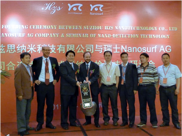 |
| Dr. Urs Matter, CEO of Nanosurf (2nd on the left) and Dr. Lukas Howald, chairman of the board for Nanosurf (4th on the left) hand over a present of �Swiss culture� to Dr. Luo, CEO of Hzs (3rd on the left). Several representatives of China�s higher education institutions and members of the Chinese Ministry of Education took part in the celebration event at Suzhou Industrial Park. |
Abstract:
Nanosurf, a leading provider of atomic force microscopes (AFM) and scanning tunneling microscopes (STM), and Suzhou Haizisi (Hzs) Nano Technology Co. Ltd., a high-tech company specialized in system solutions for nanodetection, nanofabrication and nanometrology, today announced the founding of a Sino-foreign Joint Venture, Hzs-Nanosurf (full name: Suzhou Hzs Nanosurf Nanotechnology Co. Ltd.), which after a preparation period of several months received its Chinese business license in the first half of August, 2011. The new Joint Venture represents a major milestone in the development of Nanosurf, which expects China to become one of the biggest markets for its products in the near future.
Title: Nanosurf to strengthen its position in China
Liestal, Switzerland / Suzhou, China | Posted on August 25th, 2011Located in the Suzhou Industrial Park (a Technology Park 100 km from Shanghai that offers home and office space to a residential population of more than 1 million people) and currently having a strong marketing and sales focus, Hzs-Nanosurf has all infrastructure and resources needed to become a strong Asian hub for the Nanosurf group. The joint venture will supply the full Nanosurf product range to customers in research, industry and teaching. Business is supported by a strong service, application and support center within the joint venture. "Having such strong resources in China will allow Nanosurf to gain a leading position in the research, industrial and teaching segments of this growing SPM market", comments Dr. Urs Matter, CEO of Nanosurf.
Hzs-Nanosurf is already involved in a Chinese program to provide nanotechnology teaching solutions for high schools and universities. For this purpose, an optimized version of the renowned Nanosurf STM � a scanning tunneling microscope that allows students to see atoms within minutes and of which well over a 1000 systems are operational worldwide � will be assembled at the joint venture and supplied to Chinese educational institutions. With this program, the Chinese Ministry of Education intends to provide state-of-the-art nanotechnology education to Chinese students, in order to foster their innovation capabilities in what will be one of the key technology fields of the future.
The founding of the Chinese Hzs-Nanosurf Joint Venture is part of Nanosurf's continued growth and innovation strategy: "It is a major step towards the transformation of Nanosurf into a truly global nanotechnology company", says Dr. Matter.
Nanosurf is a leading provider of user-friendly atomic force microscopes and scanning tunneling microscopes. Nanosurf products excel through their compact and elegant design, easy handling, and absolute reliability. Headquartered in Liestal, Switzerland, Nanosurf was founded in 1997 and currently has subsidiaries in Boston, USA, and in Langen, Germany. Nanosurf: Microscopy Made Easy.
Suzhou Haizisi Nano Technology Co. Ltd. designs and manufactures scanning probe microscopes that are used in education and research applications throughout China. Currently headquartered in Suzhou, China, HZS was originally founded in Shanghai in 2004. Hzs: Professional micro-nano-testing, processing and measurement solutions.
####
For more information, please click here
Contacts:
Nanosurf AG
Gr�ubernstrasse 12�14
4410 Liestal
Switzerland
Phone: +41 61 927 47 47
Fax: +41 61 927 47 00
苏州海兹思纳米科技有限公司
HZS-Nanosurf Co., Ltd.
苏州工业园区星湖街218号
纳米园A4-105
中国 China
电话:+86 512 69369060
传真:+86 512 69369055
www.hzs-nanosurf.com
Copyright © Nanosurf
If you have a comment, please Contact us.Issuers of news releases, not 7th Wave, Inc. or Nanotechnology Now, are solely responsible for the accuracy of the content.
Bookmark:


| Related News Press |
News and information
![]() Simulating magnetization in a Heisenberg quantum spin chain April 5th, 2024
Simulating magnetization in a Heisenberg quantum spin chain April 5th, 2024
![]() NRL charters Navy�s quantum inertial navigation path to reduce drift April 5th, 2024
NRL charters Navy�s quantum inertial navigation path to reduce drift April 5th, 2024
![]() Discovery points path to flash-like memory for storing qubits: Rice find could hasten development of nonvolatile quantum memory April 5th, 2024
Discovery points path to flash-like memory for storing qubits: Rice find could hasten development of nonvolatile quantum memory April 5th, 2024
Announcements
![]() NRL charters Navy�s quantum inertial navigation path to reduce drift April 5th, 2024
NRL charters Navy�s quantum inertial navigation path to reduce drift April 5th, 2024
![]() Discovery points path to flash-like memory for storing qubits: Rice find could hasten development of nonvolatile quantum memory April 5th, 2024
Discovery points path to flash-like memory for storing qubits: Rice find could hasten development of nonvolatile quantum memory April 5th, 2024
Tools
![]() Ferroelectrically modulate the Fermi level of graphene oxide to enhance SERS response November 3rd, 2023
Ferroelectrically modulate the Fermi level of graphene oxide to enhance SERS response November 3rd, 2023
![]() The USTC realizes In situ electron paramagnetic resonance spectroscopy using single nanodiamond sensors November 3rd, 2023
The USTC realizes In situ electron paramagnetic resonance spectroscopy using single nanodiamond sensors November 3rd, 2023
Alliances/Trade associations/Partnerships/Distributorships
![]() Chicago Quantum Exchange welcomes six new partners highlighting quantum technology solutions, from Chicago and beyond September 23rd, 2022
Chicago Quantum Exchange welcomes six new partners highlighting quantum technology solutions, from Chicago and beyond September 23rd, 2022
![]() University of Illinois Chicago joins Brookhaven Lab's Quantum Center June 10th, 2022
University of Illinois Chicago joins Brookhaven Lab's Quantum Center June 10th, 2022
|
|
||
|
|
||
| The latest news from around the world, FREE | ||
|
|
||
|
|
||
| Premium Products | ||
|
|
||
|
Only the news you want to read!
Learn More |
||
|
|
||
|
Full-service, expert consulting
Learn More |
||
|
|
||